Microprocessors and Microcontrollers: Unit V: (b) Introduction to RISC Based Architecture
File Register, Access Bank and Bank Switching in PIC18
Introduction to RISC Based Architecture
Review Questions 1. What is File Register in PIC18? 2. Explain the File Register data memory of PIC18F458. 3. Explain programmable memory organization of PIC18FXXX microcontroller. 4. What is access bank? 5. Explain the direct and indirect addressing methods for accessing data memory. 6. What is BSR? Explain
File Register, Access Bank and Bank Switching in PIC18
1. PIC File Register
•
In PIC18 microcontrollers, the data (Read/Write) memory is implemented as
static RAM. It is also known as File Register. Like WREG we can perform
arithmetic and logic operations on many locations of the file register data
RAM.
•
PIC microcontroller's file register size ranges from 32 bytes to several
thousands of bytes depending on the chip.
•
Fig. 2.7.1 shows the file register organization for the PIC18FXX8 devices. It
is 4096 . bytes of data memory with 12-bit address for each register.
•
The data memory map is divided into as many as 16 banks that contain 256 bytes
each. The lower 4 bits of the Bank Select Register (BSR) select which bank will
be accessed.
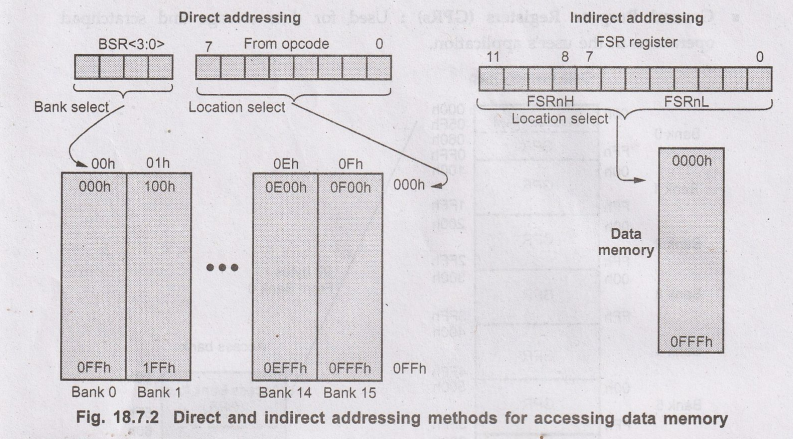
•
When using direct addressing, the Bank Select Register (BSR) is used to select
the desired bank.
•
BSR<3:0> holds the upper 4 bits of the 12-bit RAM address. These 4 bits
are used to select the desired bank. The BSR<7:4> bits will always read
'0's and writes will have no effect.
•
The file register data memory of PIC is divided into two sections :
■
Special Function Registers (SFRS): Used for control and
status of the controller and peripheral functions
■
General
Purpose Registers (GPRS): Used for data storage and
scratchpad operations in the user's application.
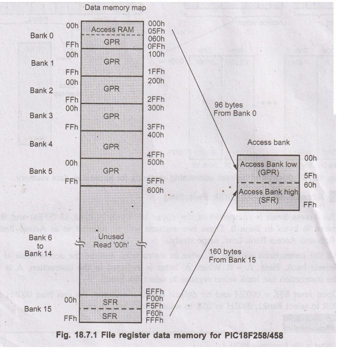
•
The SFRS start at the last location of Bank 15 (FFFh) and grow downwards. GPRS
start at the first location of Bank 0 and grow upwards.
•
The entire data memory may be accessed directly or indirectly. Direct
addressing may require the use of the BSR register. Indirect addressing
requires the use of the File Select Register (FSR). Each FSR holds a 12-bit
address value that can be used to access any location in the data memory map
without banking. Fig 18.7.2 demonstrates direct and indirect addressing
methods.
•
File Select Registers: FSRO, FSR1 and FSR2. These registers are composed of two
8-bit registers: FSRH and FSRL
2. Access Bank and Bank Switching
•
The Access Bank is comprised of the upper 160 bytes in Bank 15 (SFRS) and the
lower 96 bytes in Bank 0. These two sections will be referred to as Access Bank
High and Access Bank Low, respectively.
•
All the instructions without 'A' letter in instructions assume the access bank
as a default bank. Here, A = 0. When 'A' letter is included in the instruction,
A is 1, the instruction use bank select register to select the bank.
•
Upon reset BSR = 0000H and by default Bank0 is selected. We can load 0001H in-
BSR to select Bank1, 0002H in BSR to select Bank2 and so on.
Review Questions
1. What is File
Register in PIC18?
2. Explain the File
Register data memory of PIC18F458.
3. Explain
programmable memory organization of PIC18FXXX microcontroller.
4. What is access
bank?
5. Explain the
direct and indirect addressing methods for accessing data memory.
6. What is BSR?
Explain
Microprocessors and Microcontrollers: Unit V: (b) Introduction to RISC Based Architecture : Tag: : Introduction to RISC Based Architecture - File Register, Access Bank and Bank Switching in PIC18