Digital Logic Circuits: Unit IV: (c) Introduction to Programmable Logic Devices
FPGA (Field Programmable Gate Arrays)
Architecture block diagram, Working principle, Example Problems
• Field Programmable Gate Arrays (FPGA) provide the next generation in the programmable logic devices. The word field in the name refers to the ability of the gate arrays to be programmed for a specific function by the user instead of by the manufacturer of the device.
FPGA (Field Programmable Gate Arrays)
•
Field Programmable Gate Arrays (FPGA) provide the next generation in the
programmable logic devices. The word field in the name refers to the ability of
the gate arrays to be programmed for a specific function by the user instead of
by the manufacturer of the device. The word array is used to indicate a series
of columns and rows of gates that can be programmed by the end user.
•
As compared to standard gate arrays, the field programmable gate arrays are
larger devices. The basic cell structure for FPGA is some what complicated than
the basic cell structure of standard gate array. The programmable logic blocks
of FPGAs are called logic blocks or Configurable Logic Blocks(CLBs).
•
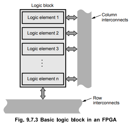
The basic architecture of FPGA consists of an array of logic blocks with
programmable row and column interconnecting channels surrounded by programmable
I/O blocks as shown in Fig. 9.7.1. Many FPGA architectures are based on a type
of memory called LUT (look-up table) rather than on (sum of product) SOP AND/OR
arrays as CPLDs are. Another approach found on some FPGAs is the use of
multiplexers to generate logic functions.

LUT
:
It is the look-up table used in FPGAs is actually a memory device that can be
programmed to perform logic functions. The LUT essentially replaces the AND/OR
array logic in a CPLD. As an example of how an LUT can be used to produce a
logic function. Fig. 9.7.2 shows a simple diagram of an 8 bit by 1 bit (8 × 1)
memory programmed to produce to SOP function 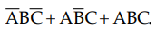 When any one of
the three product terms appears on the LUT inputs, the corresponding memory
cell storing a 1 is selected and the 1 (HIGH) appears on the output. For any
product terms that are not part of the SOP function, the LUT output is 0 (LOW).
When any one of
the three product terms appears on the LUT inputs, the corresponding memory
cell storing a 1 is selected and the 1 (HIGH) appears on the output. For any
product terms that are not part of the SOP function, the LUT output is 0 (LOW).

The
Logic Block : Each logic block in a generic FPGA
contains several logic elements, as shown in Fig. 9.7.3. Generally there can be
well over ten thousand logic elements in a single chip.
The
Logic Element : simplified diagram of a typical FPGA
logic element is shown in Fig. 9.7.4. It contains an LUT, associated logic, and
a flip-flop. In this case, each logic element contains a 4-input LUT that can
be programmed as logic function generator. It can be used to produce SOP
functions or logic functions such as adders and comparators. When configured as
an adder, the carry in and carry out allow for adder expansion. Using the
cascade logic, an LUT can be expanded by cascading with LUT's in other logic
elements. The programmable selects let you choose either combinational
functions form the LUT output or registered functions from the flip-flop
output.

Ex.
9.7.1 Explain two input LUT with implementation of the function : F (A, B) = ∑ m
(0, 3).
Sol.
:
Two input LUT has 22 × 1-bit memory, i.e. 4 × 1-bit memory. We can
implement the given function with 2-input LUT as shown in the Fig. 9.7.5.
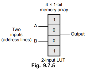
The
bit corresponding of the two-inputs of one bit wide memory array are available
at the output of LUT. For example, if inputs AB are 00, the bit from first
location is available at the output. Storing logic 1 at bit 0 and bit 3
positions, and storing logic 0 at bit 1 and bit 2 positions we can implement
the given function.
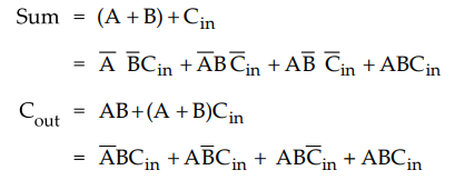
Ex. 9.7.2 Explain the three input LUT with implementation of a full adder.
Sol.
:
Fig. 9.7.6 shows an 8 × 2 LUT is programmed as a full adder. The sum and carry
out expressions for a full-adder are as follows :
Interconnection
Technology
FPGAs
use either SRAM or antifuse methods to provide interconnections between logic
blocks. The antifuse is normally open and is shorted to create a connection
when programmed, compared to the fuse which is normally shorted and is opened
to create no connection when programmed.
In
SRAM method, a transistor is controlled by the state of an on-chip SRAM cell.
When SRAM cell contains zero, the transistor is off and connection is open.
When SRAM cell contains one, the transistor is ON and connection is shorted.

Review Questions
1. Draw and explain the structural block diagram of FPGA.
2. What do you mean by FPGA ? Explain the details of internal
architecture of FPGA. How will you design any digital circuit with the help of
FPGA ?
3. With the help of structural block diagram explain FPGA with
respect to :
1) Storage cell content in LUT
2) Three input LUT
3) Inclusion of a flip-flop in an FPGA logic.
4. What is LUT in FPGA ?
5. Write a short note on FPGA.
6. Draw and explain basic architecture of FPGA. State difference
between PLA and FPGA.
7. Draw the basic structure FPGA. Explain its features in brief.
Digital Logic Circuits: Unit IV: (c) Introduction to Programmable Logic Devices : Tag: : Architecture block diagram, Working principle, Example Problems - FPGA (Field Programmable Gate Arrays)
Related Topics
Related Subjects

Digital Logic Circuits
EE3302 3rd Semester EEE Dept | 2021 Regulation | 3rd Semester EEE Dept 2021 Regulation