Electron Devices and Circuits: Unit III: (a) BJT Amplifiers
Frequency Response of an BJT Amplifier
Solved Example Problems
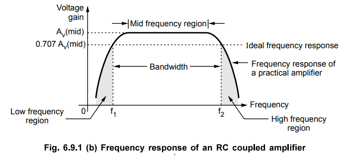
• The frequency response is nearly ideal over a wide range of mid-frequency. Only at low and high frequency ends, the gain deviates from ideal characteristics. The decrease in voltage gain with frequency is called roll-off.
Frequency Response of an Amplifier
AU
: May-04, 07, 08, 09, 11, Dec.-02, 05, 06, 08, 09, 11, 14
Concept
of Frequency Response
•
An amplifier should ideally provide the same amplification for all frequencies.
•
The degree to which this is done is usually indicated by a curve, known as
frequency response curve of the amplifier.
•
This curve is a plot of the voltage gain of an amplifier against the frequency
of input signal. A typical frequency response of an RC coupled amplifier is
illustrated in Fig. 6.9.1 (b).
•
To plot this curve, input voltage to the amplifier is kept constant and
frequency of input signal is continuously varied. The output voltage at each
frequency of input signal is noted; and the gain of the amplifier is
calculated. The output voltage or the voltage gain of the amplifier is then
plotted against frequency.
•
The frequency response is nearly ideal over a wide range of mid-frequency. Only
at low and high frequency ends, the gain deviates from ideal characteristics.
The decrease in voltage gain with frequency is called roll-off.
Cut-off
Frequencies and Bandwidth
•
To indicate how constant an amplifiers's voltage gain is with frequency
variation, we may specify the range of frequencies over which the gain does not
deviate more than 70.7 % of the maximum gain at some reference mid-frequency.
The two frequencies at which voltage gain starts decreasing below 70.7 % are
indicated by fj and f2. These are called the lower cut-off and upper cut-off
frequencies, respectively.
•
Bandwidth of the amplifier is defined as the difference between f2 and i.e.
Bandwidth of the amplifier = f2 – f1
•
The frequency f2 lies in high frequency region, while the frequency
f1 lies in low frequency region.
•
These two frequencies are also referred to as half-power frequencies since gain
or output voltage drops to 70.7 % of maximum value and this represents a power
level of one-half the power at the reference frequency in mid-frequency region.
Ex.
6.9.1 The voltage amplifier has voltage gain = 200 at cut-off frequencies. Find
the maximum voltage gain.
Sol.
: We
know that maximum voltage gain of voltage amplifier is given as,
Maximum
voltage gain = Gain at cut-off frequencies × √2 = 200 × √2 = 282.84
The
Decibel Unit
•
Usually, the voltage gain of the amplifier is represented in decibels (dBs). It
is given by,
Voltage
gain in dB = 20 log AV
For
example, assume that mid frequency gain of a certain amplifier is 100, then
Voltage
gain in dB = 20 log 100 = 20 × 2 = 40 dB
At
f1 and f2 AV = 100/√2 = 70.7
•
Voltage gain in dB at
f1
= Voltage gain in dB at f2
=
20 log 70.7 = 37 dB
•
It shows that the voltage gain at f1 and f2 is less than
3 dB of the maximum voltage gain. Due to this, frequencies f1 and f2
are also called 3 dB frequencies. The bandwidth f2 - f1
is known as 3 dB bandwidth.
•
f1 or fL is known as lower 3 dB frequency and f2 or fH is
known as upper 3 dB frequency.
Significance
of Octaves and Decades
•
The octaves and decades are the measures of change in frequency. A ten times
change in frequency is called a decade.
•
On the other hand, an octave corresponds to a doubling or halving of the
frequency. For example, an increase in frequency from 100 Hz to 200 Hz is an
octave. Likewise, a decrease in frequency from 100 kHz to 50 kHz is also an
octave.
•
At lower and higher frequencies the decrease in the gain of amplifiers is often
indicated in terms of dB/decades or dB/octaves. If the attenuation in the gain
is 20 dB for each decade, then it is indicated by line having slope of 20
dB/decade. This is illustrated in Fig. 6.9.2.
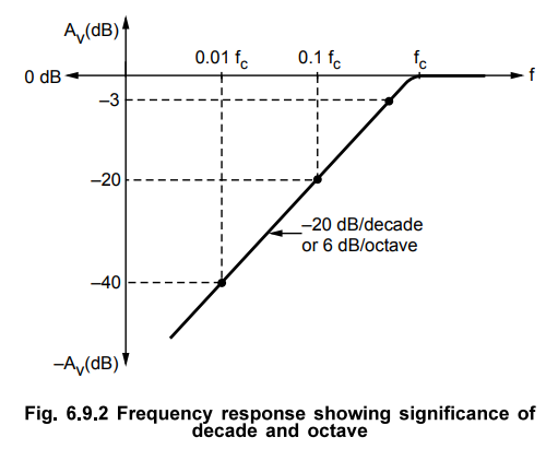
•
A rate of - 20 dB/decade is approximately equivalent to - 6 dB/octave, a rate
of - 40 dB/decade is approximately equivalent to - 12 dB/octave, and so on.
•
If the frequency is reduced to one hundredth of fc (i.e. from fc to 0.01 fc),
the drop in the voltage gain is - 40 dB. In each decade the voltage gain drops
by - 20 dB.
Midband
Gain
•
In the midband, the voltage gain of the amplifier is approximately maximum. It
is designated as midband gain or Amid.
•
The voltage gain of the amplifier outside the midband is approximately given
as,
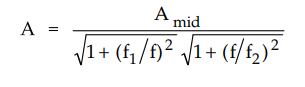
In
the midband, f1/f ≈ 0 and f/f2 ≈ 0. Therefore,
Midband
: A = Amid
Below
the midband, f/f2 = 0. As a result, the equation becomes
Below
Midband : A = Amid / √1 + (f1/f)2
Above
Midband, f1/f ≈ As a result, the equation becomes
Above
Midband : A = Amid / √1 + (f/f2)2
Ex.
6.9.2 For an amplifier, midband gain = 100 and lower cut-off frequency is 1
kHz. Find the gain of an amplifier at frequency = 20 Hz.
AU
: Dec.-14, Marks 2
Sol.
:
We know that,
Below
Midband : A = Amid / √1 + (f1/f)2
A
= 100 / √1 + ( 1000/20)2 = 2
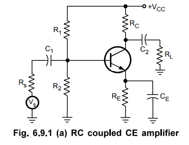
1. Effect of Various Capacitors on Frequency Response
a.
Effect of Coupling Capacitors
•
Recall that the reactance of a capacitor is Xc = 1 /2n fc. At medium and high
frequencies, the factor f makes Xc very small, so that all coupling capacitors
behave as short circuits. At low frequencies, XC increases. This increase in Xc
drops the signal voltage across the capacitor and reduces the circuit gain. As
signal frequencies decrease, the capacitor reactances increase and circuit gain
continues to fall, reducing the output voltage.
b.
Effect of Bypass Capacitors
•
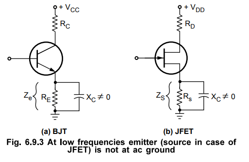
At lower frequencies, the bypass capacitor CE is not a short. So, the emitter
is not at ac ground. XC in parallel with RE (Rs in case of FET) creates an
impedance. The signal voltage drops across this impedance reducing the circuit
gain. This is illustrated in Fig. 6.9.3.
c.
Effect of Internal Transistor Capacitances
•
At high frequencies, the coupling and bypass capacitors act as short circuit
and do not affect the amplifier frequency response. However, at high
frequencies, the internal capacitances, commonly known as junction capacitances
do come into play, reducing the circuit gain.
•
Fig. 6.9.4 shows the junction capacitances for both a BJT and a JFET. In case
of the BJT, Cbe is the base emitter junction capacitance and Cbc is the base
collector junction capacitance. In case of JFET, Cgs is the internal
capacitance between gate and source and Cgd is the internal capacitance between
gate and drain.
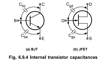
•
At higher frequencies, the reactances of the junction capacitances are low. As
frequency increases, the reactances of junction capacitances fall. When these
reactances become small enough, they provide shunting effect as they are in
parallel with junctions. This reduces the circuit gain and hence the output
voltage.
d.
Miller Theorem
•
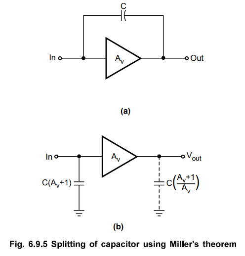
For the analysis purpose, in transistor amplifiers, it is necessary to split
the capacitance between input (base or gate) and the output (collector or
drain). This can be achieved using Miller's theorem, as shown in the Fig.
6.9.5. In Fig. 6.9.5 Av represents absolute voltage gain of the amplifier at
midrange frequencies and C represents either Cbc (in case of BJT) or Cgd (in
case of FET).
2. Low Frequency Analysis of BJT
•
Let us consider a typical common emitter amplifier as shown in Fig. 6.9.6.
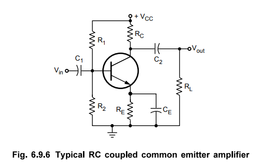
•
The amplifier shown in Fig. 6.9.6 has three RC networks that affect its gain as
the frequency is reduced below midrange. These are :
1.
RC network formed by the input coupling capacitor C and the input impedance of
the amplifier.
2.
RC network formed by the output coupling capacitor C2, the resistance looking
in at the collector, and the load resistance.
3.
RC network formed by the emitter bypass capacitor CE and the resistance looking
in at the emitter.
Input
RC Network
•
Fig. 6.9.7 shows input RC network formed by C and the input impedance of the
amplifier. Note that Vout shown in the Fig. 6.9.7 is the output voltage of the
network.
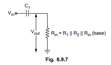
•
Applying voltage divider theorem we can write,
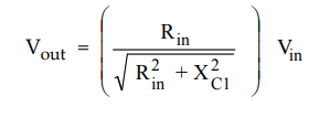
•
We know that a critical point in the amplifier response is generally accepted
to occur when the output voltage is 70.7 percent of the input (Vout = 0.707 Vin).
Thus we can write, at critical point.
R
in / √R2in + X2C1 = 0.707
= 1 / √2
At
this condition R in = XC1
•
At this condition the overall gain is reduced due to the attenuation provided
by the input RC network. The reduction in overall gain is given by,
Av
= 20 log (Vout / Vin ) = 20 log ( 0.707 )
=
- 3 dB
•
The frequency f at this condition is called lower critical frequency and is
given by,
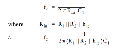
•
If the resistance of input source is taken into account the above equation
becomes
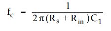
•
The phase angle in an input RC circuit is expressed as
θ
= tan-1 (XC1 / Rin)
Output
RC Network
•
Fig. 6.9.8 shows output RC network formed by C2, resistance looking in at the
collector and the load resistance.
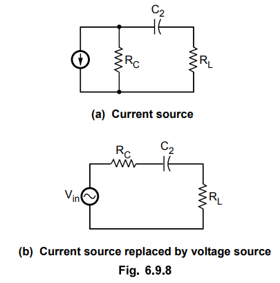
•
The critical frequency for this RC network is given by,
•
The phase angle in the output RC circuit is expressed as
θ = tan-1 (XC2 / RC + RL)
Bypass
Network
•
Fig. 6.9.9 (b) shows RC network formed by the emitter bypass capacitor CE and
the resistance looking in at the emitter.
•
Here,hie + RTH / β is the resistance looking in at the
emitter. It is derived as follows
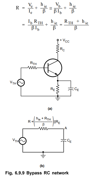
•
where RTH = R1 ||R2 ||R5. It is the
Thevenin's equivalent resistance looking from the base of the transistor
towards the input as shown in the Fig. 6.9.9 (a).
•
The critical frequency for the bypass network is
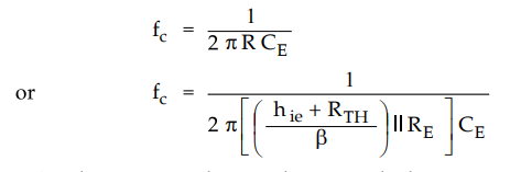
•
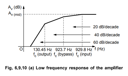
We have seen that each network has a critical frequency. It is not necessary
that all these frequencies should be equal. The network which has higher
critical frequency than other two networks is called dominant network. The
dominant network determines the frequency at which the overall gain of the
amplifier begin to drop at -20 dB/decade. This is illustrated in the following
example.
Ex.
6.9.3 Determine the low frequency response of the amplifier circuit shown in
Fig. 6.9.10.
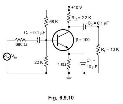
Sol.
:
It is necessary to analyze each network to determine the critical frequency of
the amplifier
a)
Input RC network :
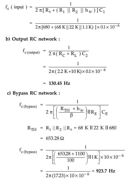
•
We have calculated all the three critical frequencies :
a)
fc (input) = 929.8 Hz
b)
fc (output) = 130.45 Hz
c)
fc (bypass) = 923.7 Hz
•
The above analysis shows that the input network produces the dominant lower
critical frequency. Fig. 6.9.10 (a) shows low frequency response of the given
amplifier.
Review Questions
1. What is bandwidth of a amplifier?
2. Explain in detail with neat diagram frequency response of BJT
amplifier. Discuss the significance of cut off frequencies and bandwidth of the
amplifier.
3. Discuss the significance of cut-off frequencies.
AU : ECE : Dec.-ll, Marks 3
4. What are the effects of coupling and bypass capacitors on the
bandwidth of the amplifier ?
AU : ECE : Dec.-02, Marks 6
5. What are the high frequency effects ?
AU : ECE : May-04, Marks 2
6. What are causes for upper cut-off frequencies in BJT?
7. What is the significance of octaves and decades in frequency
response ?
8. Derive for lower cut-off frequencies of a RC coupled BJT
amplifier.
9. Discuss the effect of bypass capacitor on frequency response
of amplifier.
10. Mention the effect of coupling capacitors on the bandwidth
of the amplifier.
Electron Devices and Circuits: Unit III: (a) BJT Amplifiers : Tag: : Solved Example Problems - Frequency Response of an BJT Amplifier
Related Topics
Related Subjects

Electron Devices and Circuits
EC3301 3rd Semester EEE Dept | 2021 Regulation | 3rd Semester EEE Dept 2021 Regulation