Linear Integrated Circuits: Unit V: Application ICs
Function Generator ICL 8038
Operating working principle, Block Diagram, Features, Circuit Diagram, Output Waveform, Pin Configuration Diagram
Function generators are designed to provide the basic waveforms such as square wave, triangular wave and sine wave. They are also called as waveform generators.
Function Generator ICL 8038
Function
generators are designed to provide the basic waveforms such as square wave,
triangular wave and sine wave. They are also called as waveform generators. The
monolithic function generators provide these basic waveforms with a minimum
number of external components reducing complexity, but increasing the
reliability of the circuit. They find application in communication, telemetry,
electronic music and testing and calibration in the laboratory.
In
function generators, VCO (voltage controlled oscillator) generates the
triangular and square waves. The triangular wave is passed through the on chip
wave shaper to generate a sine wave. The sawtooth and pulse waveforms are
generated by configuring the oscillator for a highly asymmetric duty cycle. In
this section we will discuss the ICL 8038 precision function generator from
Intersil.
1. Basic Principle
It
is very easy to understand working principle of ICL 8038 function generator
using its simplified block diagram, as shown in the Fig. 5.16.1.

The
operation of ICL 8038 is based on charging and discharging of a grounded
capacitor C, whose charging discharging rates are controlled by programmable
current generators IA and IB, respectively. When switch
is at position A, the capacitor charges at a rate determined by current source
IA . Once the capacitor voltage reaches VOT/ the upper comparator
(CMP1) triggers and resets the flip-flop output. This causes the switch
position to change from position A to B. Now, capacitor starts discharging at
the rate determined by the current sink IB.
Once
the capacitor reaches VLT, the lower comparator (CMP2) triggers and
sets the flip-flop output. This causes the switch position to change from
position B to A. And this cycle repeats. As a result, we get square wave at the
output of flip-flop and triangular wave across capacitor. The triangular wave
is then passed through the on chip wave shaper to generate sine wave.
To
allow automatic frequency control, currents IA and IB are made programmable
through an external control voltage Vi. For equal magnitudes of IA
and IB, output waveforms are symmetrical conversely, when two
currents are unequal, output waveforms are asymmetrical. By making one of the
currents much larger than other we can get sawtooth waveform across capacitor
and rectangular wave at the output of flip-flop.
2. Circuit Diagram
The
Fig. 5.16.2 shows the most simplified form of circuit diagram for ICL 8038.

As
shown in the Fig. 5.16.2, transistors Q1 and Q2 form
programmable current sources whose magnitudes are set by external resistors RA
and RB. These current sources are driven by the emitter follower
(transistor Q3). It also compensates base-emitter voltage drops for
Q1 and Q2 to ensure VRA - VRB - Vi
. Thus, IA = Vi/RA and IB = Vi/RB.
The current IA controls the charging rate of capacitor C. The
current IB is diverted to current mirror (Q4-Q5-Q6)/
where it undergoes polarity reversal as well as amplification by 2 due to the
combined action of Q5 and Q6. The result is a current
sink of magnitude of 2 IB, as shown in the Fig. 5.16.2.
The
voltage across capacitor is applied to the schmitt trigger. The schmitt trigger
shown in Fig. 5.16.2 is similar to that of the IC555, with VUT = 2/3
VCC and VLT = 1/3VCC. Transistor Q7
acts as a switch. When output of flip-flop is high, Q7 saturates and
pulls the bases of Q5 and Q6 low, thus shutting off the
current sink. As a result capacitor C starts charging at a rate set by current
IA. Once the capacitor voltage reaches 2/3 VCC(VUT),
CMP1 triggers and clears the flip-flop, thus turning Q7 off. This
enables current mirror to sink current equal to 2 IB So that net
current flowing out of the capacitor is IL = 2 IB - IA
This causes capacitor to discharge. Once
capacitor voltage reaches 1/3 VCC(VLT)/ CMP2 triggers and
sets the flip-flop and action repeats. It is important to note that net current
flowing out of capacitor C should be positive i.e. 2 IB - IA
> 0 discharging capacitor and hence 2 IB > IA.
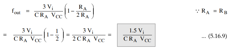
3. Frequency of Output Waveform
The
frequency of the output waveform can be determined as follows :
fout=
1/ T where T = Tc + Td
The
charging time Tc can be given as
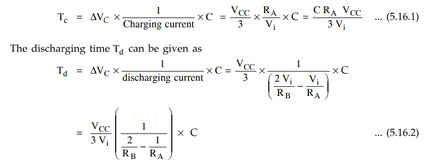
Multiplying
RA by numerator and denominator we get,
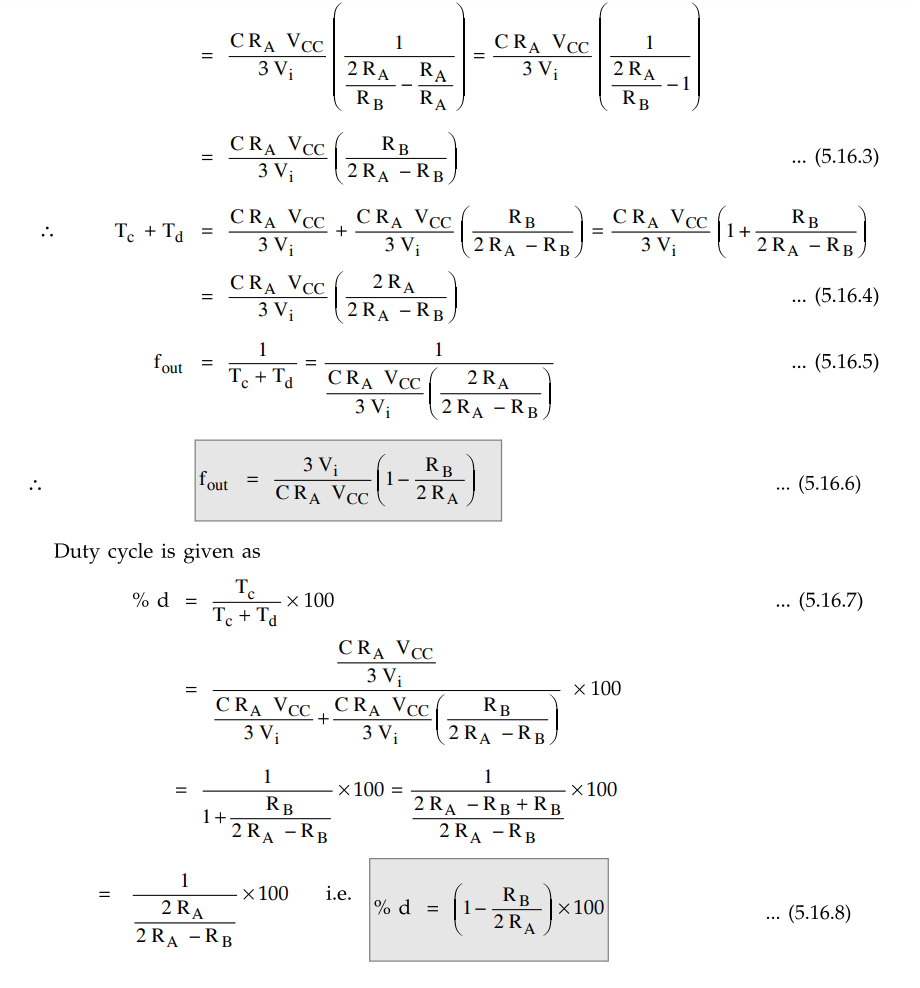
With
RA = RB, duty cycle is 50 % and we get symmetric
waveforms. For symmetric waveforms i.e. RA = RB, the
frequency of the waveform is given as,
4. Pin Configuration of ICL 8038
The
Fig. 5.16.3 shows the pin configuration for ICL 8038 function generator, which
is available in 14 pin DIP.

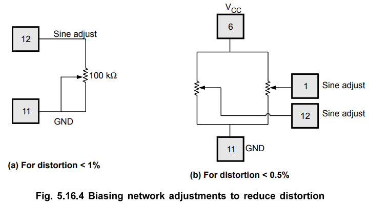
Pin
1 and Pin 12 : Sine wave adjust
The
external resistor connections to these pins decides the accuracy of the sine
wave. For distortion less than 1 % we have to connect 100 kΩ potentiometer between
pin 12 and ground or –VEE. To achieve distortion less than 0.5 % we
have to connect two 100 kΩ potentiometers between VCC and ground
with wiper of the one potentiometer connected to pin 1 and other to pin 12, as
shown in the Fig. 5.16.4.
Pin
2 : Sine wave out
The
sine wave output is available at this pin. The amplitude of sine wave is 0.22 VCC,
where ± 5V ≤ VCC ± 15 V.
Pin
3 : Traingular wave output
The
triangular wave output is available at this pin. The amplitude of triangular
wave is also function of input voltage VCC. It is 0.33 VCC
Pin
4 and 5 : Duty cycle/Frequency adjust
We
know that frequency of output is proportional to the charging and discharging
currents and duty cycle can be adjusted by selecting proper values of RA
and RB. The external resistors RA and RB are
connected to pin 4 and pin 5, respectively, as shown in the Fig. 5.16.5.
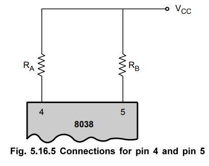
The
values of RA, RB and external capacitor connected at pin
10 decides the frequency of the output waveform. The recommended range for
values of RA and RB is from 1 kΩ to 1 MΩ.
Pin
6 : +VCC
It
is a positive supply. Its voltage should be kept between 10 V to 30 V, for a
single supply operation, and ± 5 V to ± 15 V for dual supply operation.
Pin
7 : FM bias
Refer
Fig. 5.16.2 (circuit diagram). Pin 7 is a junction of two resistors (R1 = 10 kΩ
and R2 = 40 kΩ ) that form a potential divider with the supply
voltage VCC- Looking at the same figure we can see that voltage Vj
is a voltage between VCC and pin 8. The output frequency is proportional to
this voltage. By connecting pin 7 to pin 8 the voltage across R1 appears
as a Vi. This increases the output frequency for same values of RA,
RB and C when pm 8 is connected to VCC (i.e.Vj = 0).
Pin
8 : FM sweep input
As
we know, the voltage between VCC and pin 8 decides the output
frequency. The output frequency can be controlled by applying external voltage
usually referred to as sweep voltage to pin 8. For proper operation sweep
voltage is kept between (2/3 VCC + 2) and VCC
Pin
9 : Square wave output
The
square wave output is available at this pin. As this output is open collector,
external resistor is required to be connected between VCC and pin 9
to get the square wave at pin 9.
Pin
10 : Timing capacitor
The
external timing capacitor C is connected at this pin.
Pin
11 : VEE/Ground
If
dual supply is used VEE is connected to this pin. If a single is
used, this pin is connected to the ground.
Pin
12 and 14 : Not connected
5. Typical Connection
The
Fig. 5.16.6 shows typical connection for ICL 8038 with fixed frequency and 50 %
duty cycle.

Key
Point The amplitudes of square, triangular and sine waves are VCC, 0.33
VCC and respectively. 0.22 VCC
Review Questions
1. Describe the features and one application of function
generator IC.
May-05, Dec.-05, Marks 16
2. Draw the block diagram of the function generator ICL 8038 or
any other equivalent and explain its operation.
May-04,11,15, Marks 16, Dec.-08,09,ll, Marks 16
3. Write short note on ICL 8038 function generator.
Dec.-16, 17, May-16, 17, Marks 8
Linear Integrated Circuits: Unit V: Application ICs : Tag: : Operating working principle, Block Diagram, Features, Circuit Diagram, Output Waveform, Pin Configuration Diagram - Function Generator ICL 8038
Related Topics
Related Subjects

Linear Integrated Circuits
EE3402 Lic Operational Amplifiers 4th Semester EEE Dept | 2021 Regulation | 4th Semester EEE Dept 2021 Regulation