Linear Integrated Circuits: Unit V: Application ICs
General Purpose Linear IC 723 Regulator
Pin diagram, Important Features, Internal Structure, Functional Block Diagram, Applications, Solved Example Problems
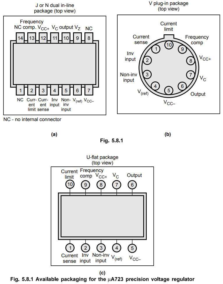
The popular general purpose precision regulator is IC 723. It is a monolithic linear integrated circuit in different physical packages.
General Purpose Linear IC 723 Regulator
Dec.-03,04,05,06,07,08,10,12,14,15,
May-07,08,12,13,14
The
popular general purpose precision regulator is IC 723. It is a monolithic
linear integrated circuit in different physical packages.
The
pin diagram alongwith the various packages is shown in the Fig. 5.8.1 (a), (b)
and (c).
1. Important Features of IC 723
1)
It works as voltage regulator at output voltage ranging from 2 to 37 volts at
currents upto 150 mA.
2)
It can be used at load currents greater than 150 mA with use of suitable NPN or
PNP external pass transistors.
3)
Input and output short-circuit protection is provided.
4)
It has good line and load regulation (0.03 %)
5)
Wide variety of applications of series, shunt, switching and floating
regulator.
6)
Low temperature drift and high ripple rejection.
7)
Low standby current drain.
8)
Small size, lower cost
9)
Relative ease with which power supply can be designed.
10)
It provides a choice of supply voltage.
2. Internal Structure of IC 723
The
functional block diagram of IC 723 can be divided into four major blocks
1)
Temperature compensated voltage reference source, which is zener diode.
2)
An op-amp circuit used as an error amplifier.
3)
A series pass transistor capable of a 150 mA output current.
4)
Transistor used to limit output current.
The
functioning of the above blocks can be explained with the help of a simplified
functional block diagram of IC 723 as shown in the Fig. 5.8.2.
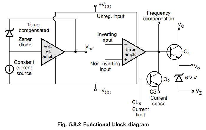
Temperature
compensated zener diode, constant current source and reference amplifier
constitutes the reference element.
Key
Point In order to get a fixed voltage from zener
diode, the constant current source forces the zener to operate at a fixed
point.
Output
voltage is compared with this temperature compensated reference potential of
the order of 7 volts. For this, Vref is connected to the
non-inverting input of the error amplifier.
This
error amplifier is high gain differential amplifier. It's inverting input is
connected to the either whole regulated output voltage or part of that from
outside. For later case a potential divider of two scaling resistors is used. Scaling
resistors help in getting multiplied reference voltage or scaled up reference
voltage.
Error
amplifier controls the series pass transistor Q1 which acts as
variable resistor. The series pass transistor is a small power transistor
having about 800 mW dissipation. The unregulated power supply source (< 36 V
d.c.) is connected to collector of series pass transistor.
Transistor
Q2 acts as current limiter in case of short circuit condition. It
senses drop across Rsc placed in series with regulated output
voltage externally.
The
frequency compensation terminal controls the frequency response of the error
amplifier. The required roll-off is obtained by connecting a small capacitor of
100 pF between frequency compensation and inverting input terminals.
The
internal structure can be represented in more simplified form as shown in the
Fig. 5.8.3.
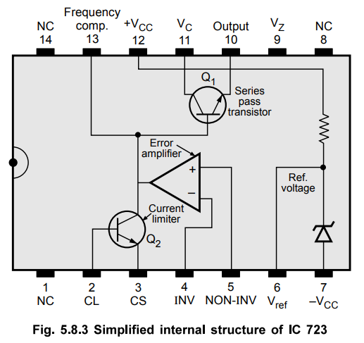
Both
noninverting and inverting terminals of the error amplifier are available on
outside pins of IC 723. Due to this, device becomes versatile and flexible to
use. Only restriction is that internal reference voltage is 7 volts and
therefore we have to use two different circuits for getting regulated outputs
of below 7 volts and above 7 volts.
3. Applications of IC 723
The
various regular circuits as per the requirement can be achieved using IC 723.
Some of them are discussed below :
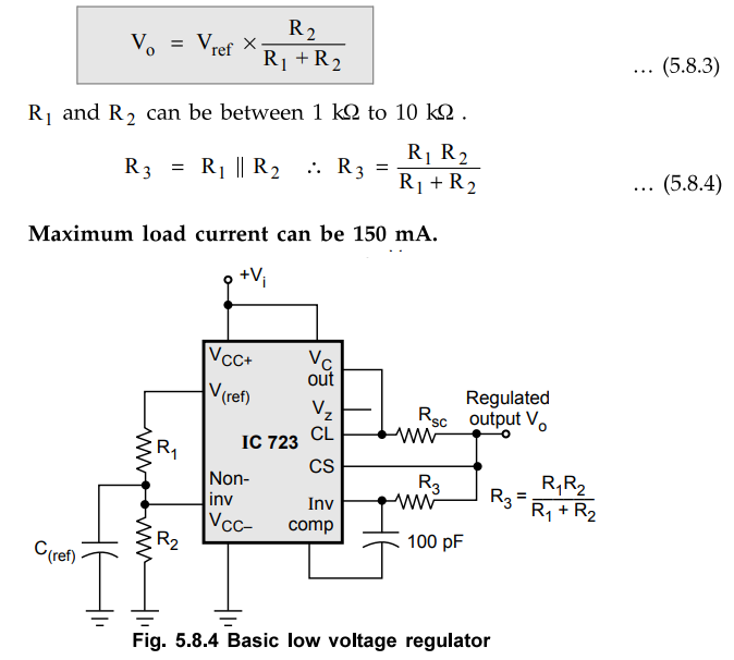
a.
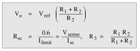
Basic Low Voltage Regulator (Vo = 2 to 7 volts)
The
resistor, Rsc is connected between CL and CS pins. The current limit
transistor remains non-conductive unless drops across Rsc is 0.6 V
(equal to VBE drop). The value of Rsc can be found out by
following equation
Rsc
= Vsense / Ilimit = 0.6 / Ilimit …. (5.8.1)
Ilimit
can be selected as 1.2 to 1.5 times the maximum load circuit. Potential divider
made up of R1 and R2 is connected between Vref and
non-inverting terminals.
Vnon
–inverting = Vref × R2 / R1 + R2
... (5.8.2)
As
the series pass transistor is working as emitter follower.
b.
Low Voltage High Current Regulator
Output
voltage from +2 to +7V and load current can be more than 150 mA. For this one
transistor is connected externally, shown as Q1 in the Fig. 5.8.5.
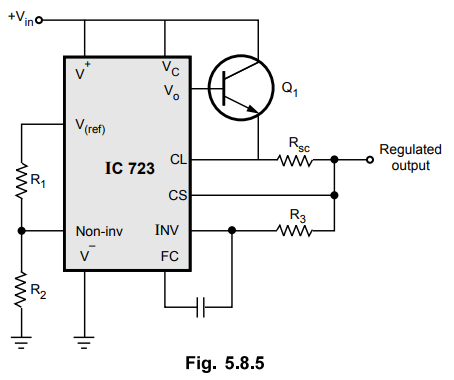
The
functional equations are similar to that of basic low voltage regulator
circuit.
c.
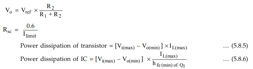
Basic Positive High Voltage Regulator
For
this type, output voltage varies from +7 V to +37 V and IL ≤ 150 mA.
The
non-inverting terminal connected to Vref through R3. Due to this arrangement
the error amplifier acts as non-inverting amplifier.
This
is also called basic high voltage low current regulator.
d.
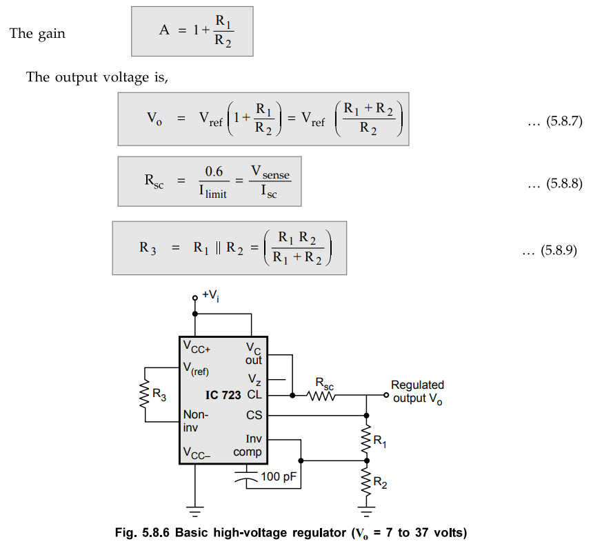
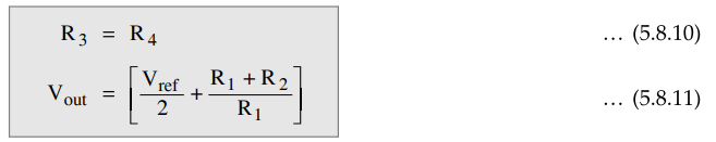
Positive High Voltage High Current Regulator
For
this type, output voltage from +7 V to +37 V and load current IL
> 150 mA. For this a external transistor Q1 is connected, as
shown in the Fig.5.8.7.
For
this different expressions are similar to basic high voltage regulator and
reproduced for the convenience.
While
the power dissipation of transistor Q1 and the IC is given by the same
expressions as given by the equations (5.8.5) and (5.8.6).
e.
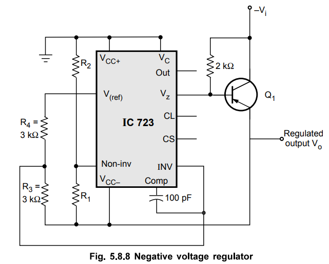
Negative Voltage Regulator
Connections
for getting negative voltage regulator are shown in Fig. 5.8.8. An external PNP
transistor, Q1 is connected. Resistances can be from 1 kΩ to 10 kΩ
If
magnitude of -Vi is less than 9 V, connect VCC+ and VC
to a positive supply such that VCC+ to VCC- is greater
than 9 V, for proper functioning of the IC.
Example
5.8.1 Design a regulator using IC 723 to meet the
following specifications :
Vo
= 5 V; Io = 100mA. Vin = 15 ± 20 %
Isc
= 150 mA; Vsense = 0.7 V
Solution
:
The given specifications are, Vo = 5 V; Io = 100 mA, Vin
= 15 ± 20 %,
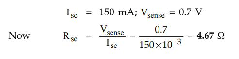
Neglecting
input bias current of an error amplifier we can write,
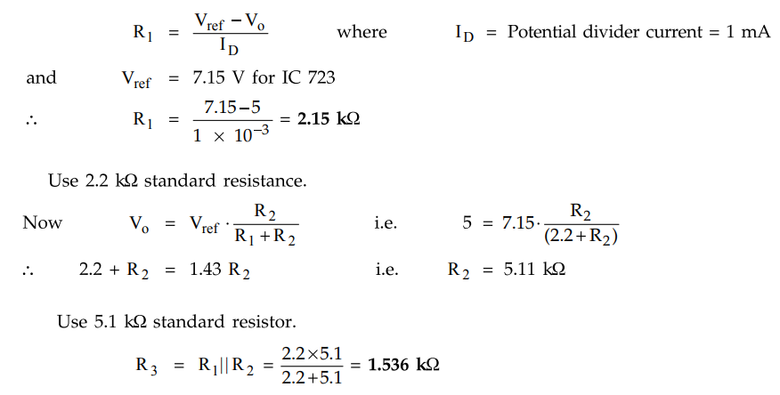
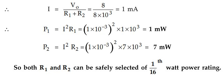
Use
1.5 kΩ (standard) resistor.
The
designed regulator is shown in the Fig. 5.8.9.
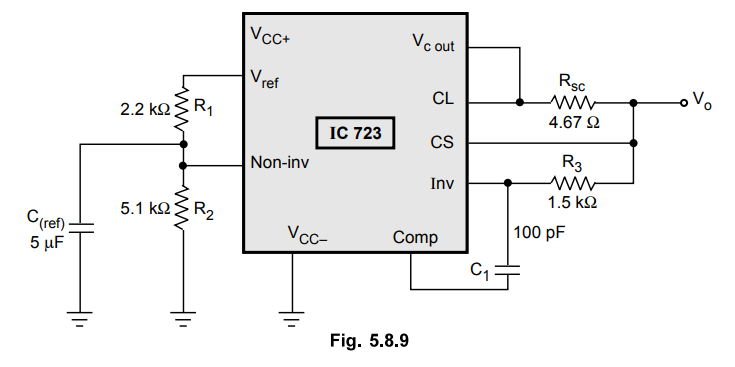
Example
5.8.2 Draw the circuit diagram of IC 723 based
positive voltage regulator, to give + 8 V output at 200 mA. Incorporate short
circuit protection current limit circuit to operate at 400 mA. Find all
resistor values and calculate their wattage.
Solution
:
Vo = + 8 V,
IL
= 200 mA, Isc = 400 mA
As
output is more than 7 V and IL is more than 150 mA, it is positive high voltage
high current regulator. It is shown in the Fig. 5.8.10.
The
equations of operation are,
All
the resistor type can be of metal film resistors.
For
the power rating of R1 and R2, assume the input current
to the inverting terminal zero.
Example
5.8.3 Design an adjustable voltage regulator (5 V to
15 V) with a short circuit current limit of 50 mA using a 723 regulator.
Solution
:
Let us design it as a basic high voltage regulator but by changing Vref
from 7 V to V'ref less than 5 V. The circuit is shown in the Fig.
5.8.11.
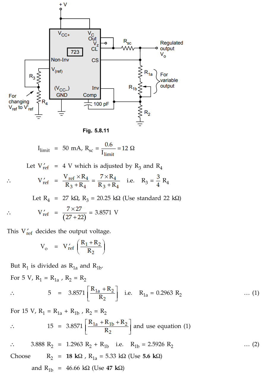
By
varying R1b, continuous adjustment of Vo from 5 V to 15 V
can be achieved.
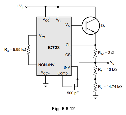
Example
5.8.4 Design a voltage regulator using IC 723
regulator to satisfy the following specifications :
i)
Vo = 12V, ii) Io -
500 mA, iii) Vin = 18 + 20 % iv)
Isc = 600 mA,
and.
v) Vsense = 0.7 V. Give the complete schematic diagram. (Assume and
justify if any data required)
Solution
:
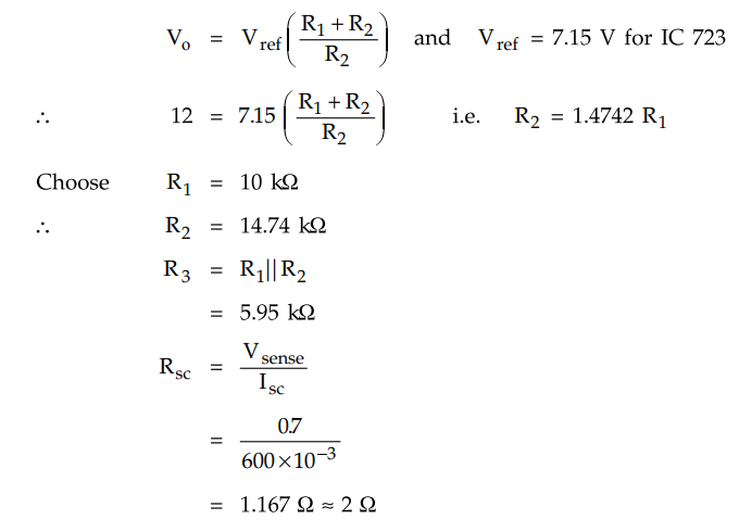
The
output transistor is required to satisfy
Io
= 500 mA
The
designed circuit is shown in the Fig. 5.8.12.
Review Questions
1. List the important
features of IC 723.
2. Explain the
following applications of IC723,
i. Basic low voltage
regulator
ii. Basic positive
high voltage regulator.
3. Discuss the
internal structure of 723 voltage regulator.
4. Design a low
voltage regulator using 723 for 5 V and explain its characteristics.
Dec.-05, Marks 8
5. Explain the current
limiting feature and current boosting in 723 IC.
May-08, Marks 10
6. Draw and explain
the functional block diagram of a 723 IC regulator and make the necessary
changes to make it as low voltage regulator.
Linear Integrated Circuits: Unit V: Application ICs : Tag: : Pin diagram, Important Features, Internal Structure, Functional Block Diagram, Applications, Solved Example Problems - General Purpose Linear IC 723 Regulator
Related Topics
Related Subjects

Linear Integrated Circuits
EE3402 Lic Operational Amplifiers 4th Semester EEE Dept | 2021 Regulation | 4th Semester EEE Dept 2021 Regulation