Electron Devices and Circuits: Unit I: PN Junction Devices
Half Wave Rectifier
Circuit Diagram, Operations, Calculation, Formula, Advantages, Disadvantages, Solved Example Problem
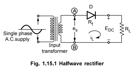
• In half wave rectifier, rectifying element conducts only during positive half cycle of input a.c. supply. The negative half cycles of a.c. supply are eliminated from the output.
Half Wave Rectifier
AU
: May-11,12, Dec.-15, 16
•
In half wave rectifier, rectifying element conducts only during positive half
cycle of input a.c. supply. The negative half cycles of a.c. supply are eliminated
from the output.
•
This rectifier circuit consists of resistive load, rectifying element, i.e. p-n
junction diode, and the source of a.c. voltage, all connected in series. The
circuit diagram is shown in the Fig. 1.15.1. Usually, the rectifier circuits
are operated from a.c. mains supply. To obtain the desired d.c. voltage across
the load, the a.c. voltage is applied to rectifier circuit using suitable
step-up or step-down transformer, mostly a step-down one, with necessary turns
ratio.
•
The input voltage to the half-wave rectifier circuit shown in the Fig. 1.15.1
is a sinusoidal a.c. voltage, having a frequency which is the supply frequency,
50 Hz.
•
The transformer decides the peak value of the secondary voltage. If Nj are the
primary number of turns and N2 are the secondary number of turns and Epm is the
peak value of the primary voltage then,
N2
/ N1 = Eam / Epm
•
Where Epm = The peak value of the secondary a.c. voltage.
•
As the nature of is sinusoidal the instantaneous value will be,
es
= Esm sin ωt
where ω = 2π f and f = Supply frequency
•
Let Rf represents the forward resistance of the diode. Assume that,
under reverse biased condition, the diode acts almost as an open circuit,
conducting no current.
1. Operation of the Circuit
•
During the positive half cycle of secondary a.c voltage, terminal (A) becomes
positive with respect to terminal (B). The diode is forward biased and the
current flows in the circuit in the clockwise direction, as shown in the Fig.
1.15.2 (a). The current will flow for almost full positive half cycle. This
current is also flowing through load resistance RL hence denoted as
iL, the load current.
•
During negative half cycle when terminal (A) is negative with respect to
terminal (B), diode becomes reverse biased. Hence no current flows in the
circuit as shown in the Fig. 1.15.2 (b). Thus the circuit current, which is
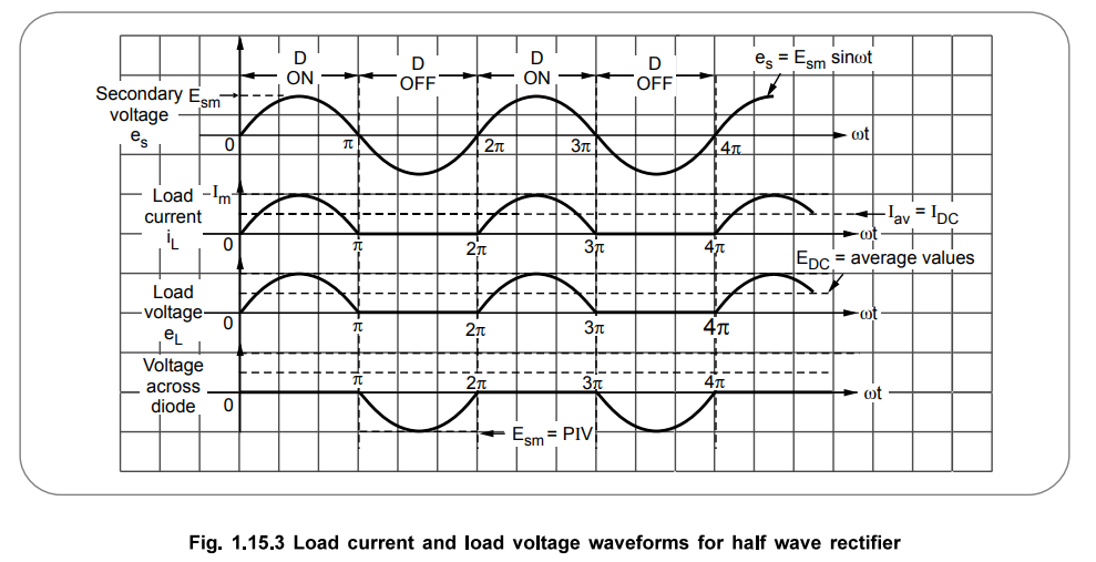
also the load current, is in the form of half sinusoidal pulses.

•
The load voltage, being the product of load current and load resistance, will
also be in the form of half sinusoidal pulses. The different waveforms are
illustrated in Fig. 1.15.3.
•
The d.c. output waveform is expected to be a straight line but the half wave
rectifier gives output in the form of positive sinusoidal pulses.
Key
Point : Hence the output is called pulsating d.c. It is
discontinuous in nature. Hence it is necessary to calculate the average value
of load current and average value of output voltage.
2. Average D.C. Load
Current (lDC)
•
The average or d.c. value of alternating current is obtained by integration.
•
For finding out the average value of an alternating waveform, we have to
determine the area under the curve over one complete cycle i.e. from 0 to 2n
and then dividing it by the base i.e. 2π .
•
Mathematically, current waveform can be described as,
iL
= Im sin ωt for 0 ≤ ωt
≤ π
iL
= 0 for π ≤ ωt ≤ 2π
where Im = Peak value of load
current
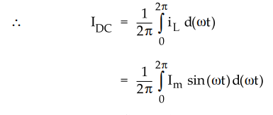
•
As no current flows during negative half cycle of a.c. input voltage, i.e.
between ωt = π to ωt = 2 π, we change the limits of integration.
•
where RS = Resistance of secondary winding of transformer. If RS
is not given it should be neglected while calculating Im .
3. Average D.C. Load Voltage (EDC)
•
It is the product of average D.C. load current and the load resistance RL.
EDC
= IDCRL
•
Substituting value of IDC,
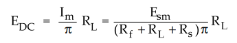
•
The winding resistance Rs and forward diode resistance Rf are practically very
small compared to RL
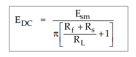
•
But as Rf and Rg are small compared to RL , (Rf + RS)/RL is negligibly small
compared to 1. So neglecting it we get,
EDC
≈ Esm / π
Note
:
When Rf and Rg are finite, calculate Im, then IDC and from that calculate EDC
as IDCRL
Key
Point : Do not calculate EDC as Esm / π directly
for finite R, and R . Calculate Im then IDC and then EDC
as IDCRL
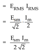
4. R.M.S. Value of Load Current (IRMS)
The
R.M.S means squaring, finding mean and then finding square root. Hence R.M.S.
value of load current can be obtained as,
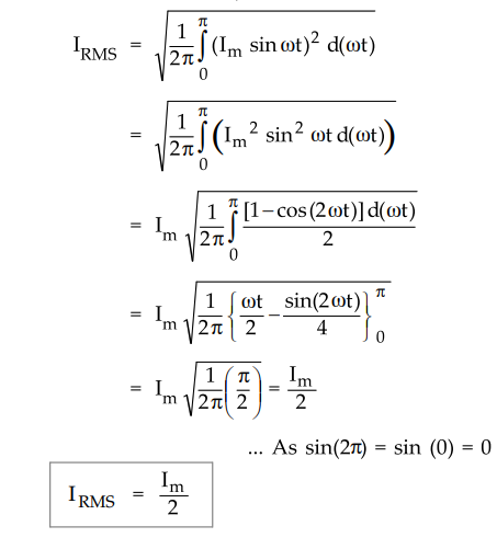
Note
:
Students must remember that this R.M.S. value is for half wave rectified
waveform hence it is Im/2. For full sine wave it is Im/√2 which is derived later.
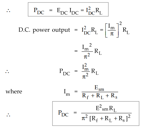
5. D.C. Power Output (PDC)
The
d.c. power output can be obtained as,
6. A.C. Power Input (PAC)
The
power input taken from the secondary of transformer is the power supplied to
three resistances namely load resistance RL , the diode resistance
Rf and winding resistance RS. The a.c. power is given by,

7. Rectifier Efficiency
•
The rectifier efficiency is defined as the ratio of output d.c. power to input
a.c. power.
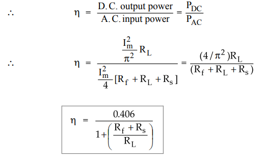
•
If (Rf + Rs) << RL as mentioned earlier, we get the maximum
theoretical efficiency of half wave rectifier as,
%
ηmax = 0.406 × l0° = 40.6 %
•
Thus in half wave rectifier, maximum 40.6 % a.c. power gets converted to d.c.
power in the load. If the efficiency of rectifier is 40 % then what happens to
the remaining 60 % power. It is present interms of ripples in the output which
is fluctuating component present in the output.
Key
Point : Thus more the rectifier efficiency, less are the
ripple contents in the output.
8. Ripple Factor (ɤ)
•
It is seen that the output of half wave rectifier is not pure d.c. but a
pulsating d.c. The output contains pulsating components called ripples. Ideally
there should not be any ripples in the rectifier output. The measure of such
ripples present in the output is with the help of a factor called ripple factor
denoted by ɤ It tells how smooth is the output.
Key
Point : Smaller the ripple factor closer is the
output to a pure d.c.
•
The ripple factor expresses how much successful the circuit is, in obtaining
pure d.c. from a.c. input.
Definition
:
•
Mathematically ripple factor is defined as the ratio of R.M.S. value of the
a.c. component in the output to the average or d.c. component present in the
output.
Ripple
factor
ɤ
= R.M.S. value of a.c. component of
output / Average or d.c. component of output
•
Now the output current is composed of a.c. component as well as d.c. component.
Let Iac = R.M.S. value of a.c.
component present in output
IDC
= D.C. component present in output
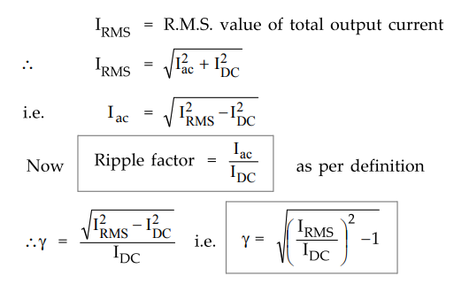
•
This is the general expression for ripple factor and can be used for any
rectifier circuit.
•
Now for a half wave circuit,
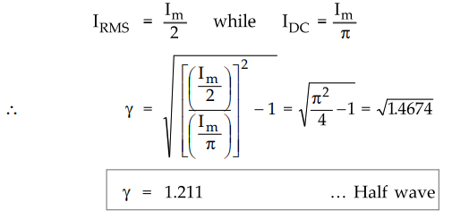
•
This indicates that the ripple contents in the output are 1.211 times the d.c.
component i.e. 121.1 % of d.c. component.
Key
Point : The ripple factor for half wave is very high
which indicates that the half wave circuit is a poor converter of a.c. to d.c.
•
The ripple factor is minimised using filter circuits along with the rectifiers.
9. Load Current
•
The load current iL which is composed of a.c. and d.c. components
can be expressed using Fourier series as,
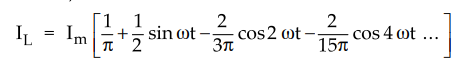
•
This expression shows that the current may be considered to be the sum of an
infinite number of current components, according to Fourier series.
•
The first term of the series is the average or d.c. value of the load current.
The second term is a varying component having frequency same as that of a.c.
supply voltage. This is called fundamental component of the current having
frequency same as the supply. The third term is again a varying component
having frequency twice the frequency of supply voltage. This is called second
harmonic component. Similarly all the other terms represent the a.c. components
and are called harmonics.
•
Thus ripple in the output is due to the fundamental component along with the
various harmonic components. And the average value of the total pulsating d.c.
is the d.c. value of the load current, given by the constant term in the
series, Im / π.
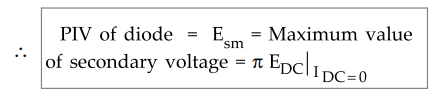
10. Peak Inverse Voltage (PIV)
•
The Peak Inverse Voltage is the peak voltage across the diode in the reverse
direction i.e. when the diode is reverse biased. In half wave rectifier, the
load current is ideally zero when the diode is reverse biased and hence the
maximum value of the voltage that can exist across the diode is nothing but
Egm. This is shown in the Fig. 1.15.4.
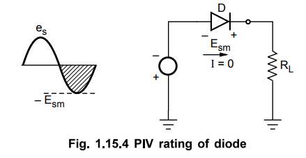
•
Thus PIV occurs at the peak of each negative half cycle of the input, when
diode is reverse biased and not conducting.
•
This is called PIV rating of a diode. So diode must be selected based on this
PIV rating and the circuit specifications.
11. Transformer Utilization Factor (T.U.F.)
•
The factor which indicates how much is the utilization of the transformer in
the circuit is called Transformer Utilization Factor (T.U.F.)
Definition
:
•
The T.U.F. is defined as the ratio of d.c. power delivered to the load to the
a.c power rating of the transformer. While calculating the a.c. power rating,
it is necessary to consider r.m.s. value of a.c. voltage and current.
•
The T.U.F. for half wave rectifier can be obtained as,
A.C.
power rating of transformer =
•
Remember that the secondary voltage is purely sinusoidal hence its r.m.s. value
is 1/V2 times maximum while the current is half sinusoidal hence its r.m.s.
value is 1/2 of the maximum, as derived earlier.
D.C.
power delivered to the load =

Key
Point : The value of T.U.F. is low which shows
that in half wave circuit, the transformer is not fully utilized.
12. Voltage Regulation
•
The secondary voltage should not change with respect to the load current. The
voltage regulation is the factor which tells us about the change in the d.c.
output voltage as load changes from no load to full load condition.
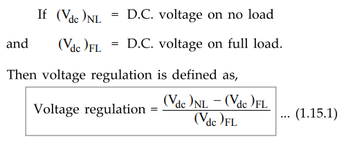
Key
Point : Less the value of voltage regulation, better is
the performance of rectifier circuit.
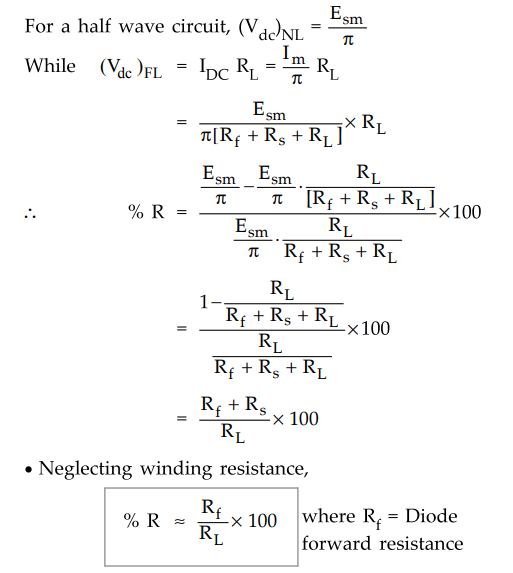
Key
Point : Ideally the load regulation is zero as ideal
value of Rf is zero in forward biased condition.
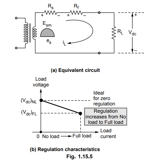
a.
Regulation Characteristics
•
Consider the equivalent circuit of the half wave rectifier, for positive half
cycle of the transformer secondary voltage as shown in the Fig. 1.15.5 (a).
•
As load current increases (RL decreases), the drop across Rg and Rf goes on
increasing, but the transformer, secondary voltage remains same. Hence the d.c.
output voltage decreases. Hence load voltage decreases as load changes from no
load to full load. To keep the drop across Rg and Rf minimum, values of Rg and
Rf. must be as small as possible. The graph of load voltage against load
current is called regulation characteristics which is drooping in nature as
shown in the Fig. 1.15.5 (b).
13. Advantages of Half Wave Rectifier
1.
Only one diode is sufficient.
2.
Easy to design.
3.
Centre tap transformer is not required.
14. Disadvantages of Half Wave Rectifier Circuit
•
The various disadvantages of the half wave rectifier circuit are,
1.
The ripple factor of half wave rectifier circuit is 1.21, which is quite high.
The output contains lot of varying components.
2.
The maximum theoretical rectification efficiency is found to be 40 %. The
practical value will be less than this. This indicates that half wave rectifier
circuit is quite inefficient.
3.
The circuit has low transformer utilization factor, showing that the
transformer is not fully utilized.
4.
The d.c. current is flowing through the secondary winding of the transformer
which may cause dc saturation of the core of the transformer. To minimize the saturation, transformer size
have to be increased accordingly. This increases the cost.
•
Because of all these disadvantages, the half-wave rectifier circuit is normally
not used as a power rectifier circuit.
•
Due to the barrier potential of 0.7 V for Si diode, the peak value of the
output is 0.7 V less than peak value of the input voltage.
VP
(output) = Esm - 0.7V
•
This effect is generally neglected as peak value of the input voltage is much
greater than the barrier potential of 0.7 V. For Ge diodes, barrier potential
is about 0.2 V which is very small and practically neglected.
Ex.
1.15.1 A half wave rectifier circuit is supplied from a 230 V, 50 Hz supply
with a step down ratio of 3 : 1 to a resistive load of 10 fcQ. The diode
forward resistance is 75 Q while transformer secondary resistance is 10 Q.
Calculate maximum, average, RMS values of current, D.C. output voltage,
efficiency of rectification, regulation and ripple factor.
Sol.
:
The circuit is shown in the Fig. 1.15.6.
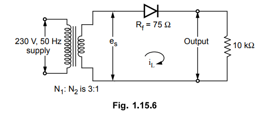
•
The given values are,
Rf
= 75 Ω, RL = 10 k Ω, Rs = 10 Ω.
•
The given supply voltages are always r.m.s. values.
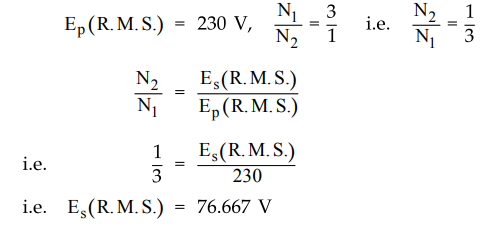
•
This is r.m.s. value of the transformer secondary voltage.

Review Questions
1. What is half wave rectifier ? Explain the working principle
with neat sketch.
AU : May-11, Dec.-15, 16, Marks 8
2. Derive the expressions for the following parameters of the
half wave rectifier circuit :
a. Average d.c. current (IDC)
b. Average d.c. voltage (EDC)
c. R.M.S. value of current (IRMS)
d. D.C. power output (PDC)
e. A.C. power input (PAC)
f. Rectifier efficiency (η)
g. Ripple factor (ɤ).
AU : Dec.-16, Marks 8
3. Define the following terms
i) Transformer utilization factor
ii) Ripple factor of HWR with resistive load and derive the
expression for the same.
4. What are the disadvantages of a half wave rectifier circuit ?
5. Show that for a half wave circuit
%η = 40.6 / (1 + Rf/RL) % where Rf
is forward resistance of diode and RL is the load resistance.
6. Draw the circuit diagram of half-wave rectifier and explain
it's operation with necessary wave form. Also derive expression for
rectification efficiency and transformer utilisation factor.
AU : May-12, Marks 10
7. A voltage V = 300 cos 1001 is applied to a half wave
rectifier, with RL = 5kti. The rectifier may be represented by ideal diode in
series with a resistance of lkΩ,. Calculate
i) Im ii) D.C.
power iii) A.C. power iv) Rectifier efficiency and v) Ripple factor.
[Ans.: 50 mA, 1.2665 watts, 3.75 watts, 33.77 %, 1.211]
Electron Devices and Circuits: Unit I: PN Junction Devices : Tag: : Circuit Diagram, Operations, Calculation, Formula, Advantages, Disadvantages, Solved Example Problem - Half Wave Rectifier
Related Topics
Related Subjects

Electron Devices and Circuits
EC3301 3rd Semester EEE Dept | 2021 Regulation | 3rd Semester EEE Dept 2021 Regulation