Microprocessors and Microcontrollers: Unit I: (e) I/O Interfacing
I/O Interfacing Techniques in 8085
The most of the microprocessors support isolated I/O system. It partitions memory from I/O, via software, by having instructions that specifically access (address) memory, and others that specifically access I/O.
I/O Interfacing Techniques in 8085
AU
: May-04, 05, 06, 07, 12, 16, Dec.-04, 05, 09, 10, 12
The
most of the microprocessors support isolated I/O system. It partitions memory
from I/O, via software, by having instructions that specifically access
(address) memory, and others that specifically access I/O. When these
instructions are decoded by the microprocessor, an appropriate control signal is
generated to activate either memory or I/O operation. In 8085,  signal is used for this purpose. The 8085 outputs a logic '1' on the line for an I/O operation and a logic 'O' for memory operation. In 8085, it is
possible to connect 64 kbyte memory and 256 I/O ports in the system since 8085
sends 16 bit address for memory and 8-bit address for I/O. I/O devices can be
interfaced to an 8085A system in two ways :
signal is used for this purpose. The 8085 outputs a logic '1' on the line for an I/O operation and a logic 'O' for memory operation. In 8085, it is
possible to connect 64 kbyte memory and 256 I/O ports in the system since 8085
sends 16 bit address for memory and 8-bit address for I/O. I/O devices can be
interfaced to an 8085A system in two ways :
1.
I/O Mapped I/O 2. Memory mapped I/O
1. I/O Mapped I/O
In
I/O mapped I/O, the 8085 uses signal to distinguish between I/O
read/write and memory read/write operations. The 8085 has separate instructions
IN and OUT for I/O data transfer. When 8085 executes IN or OUT instruction, it
places device address (port number) on the demultiplexed low order address bus
as well as the high order address bus. In other words, we can say that higher
order address bus duplicates the contents of demultiplexed low-order address
bus, when 8085 microprocessor executes an IN or OUT instruction. For example,
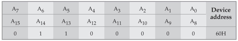
if the device address is 60H then the contents on A15 to A0
will be as follows :
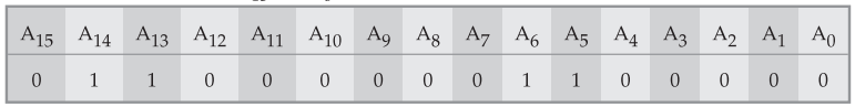
Here,
A8 follows A0, A9 follows A1 and so
on, as shown below.
The
instruction IN inputs data from an input device (such as keyboard) into the
accumulator and the instruction OUT sends the contents of the accumulator to an
output device such as LED display. These are two byte instructions. The second
byte of the instruction specifies the address or the port number of an I/O
device. As it is a byte, the address or port number can be any of the 256
combinations of eight bits, from OOH to FFH. Therefore, the 8085 can
communicate with 256 different I/O devices. When we want to interface an I/O
device, it is necessary to assign a device address or a port number. Before
going to see this device address logic, we will examine how the 8085 executes
IN and OUT instructions.
IN
and OUT instructions :
IN
:
It
is used to read 8-bit data from I/O device into the accumulator. This two byte
instruction has, the first byte as an opcode and the second byte specifies the
device address or a port number.
2. I/O Device Selection
As
mentioned earlier, the 8085 gives 8-bit I/O address. This means it can select
one of the 256 I/O ports. To select an appropriate I/O device, it is necessary
to do following things.
1.
Decode the address to generate unique signal corresponding to the device
address on the bus.
2.
When device address signal and control signal  both are low, generate
device select signal.
both are low, generate
device select signal.
3.
Use device select signal to activate the interfacing device (I/O port).
Fig. 7.2.1 shows the absolute decoding circuit
for the I/O device. The IC 74LS138, 3:8 decoder along with 3 input OR gate is
used to generate device select signal. This signal is ORed with signal to generate device enable signal.
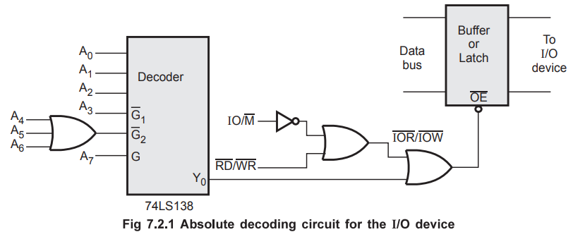
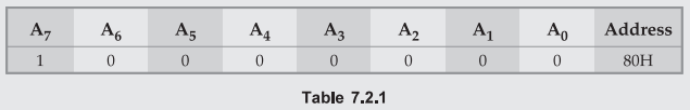
To
generate device select signal (Y0) low, the address on the address
bus must be as given below :
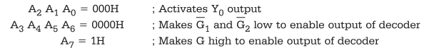
Key
Point Decoder output is enabled only when control
signals  are low and control signal G is high. Therefore the address
of this I/O device is 80H as shown in the Table 7.2.1. Table 7.2.1
are low and control signal G is high. Therefore the address
of this I/O device is 80H as shown in the Table 7.2.1. Table 7.2.1
3. Interfacing Input and Output Devices with Examples
Interfacing
Input Device :
The microprocessor 8085 accepts 8-bit data from the input device such as keyboard, sensors, transducers etc. Fig. 7.2.2 shows the circuit diagram to interface input port (buffer) which is used to read the status of 8 switches. The address for this input device is 80H as device select signal goes low when address is 80H.

When
the switch is in the released position, the status of line is high otherwise
status is low. With this information microprocessor can check a particular key
is pressed or not.
The
following program checks whether the switch 2 is pressed or not.
Program
:
IN
SOH ; Read status of all switches
ANI
02H ; Mask bit positions for other switches
JZ
NEXT ; if program control is transferred to label
;
NEXT, then switch 2 is pressed otherwise not.
Interfacing
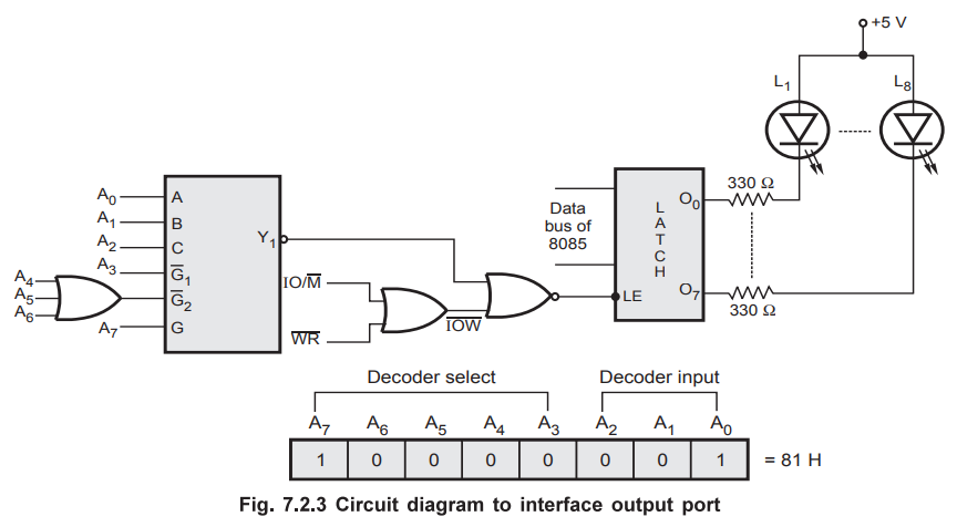
Output Device :
The
microprocessor 8085 sends 8-bit data to the output device such as 7 segment
displays, LEDs, printer etc. Fig 7.2.3 shows the circuit diagram to interface
output port (latch) which is used to send the signal for glowing the LEDs. LED
will glow when output pin status is low. The IC 74LS138 and 3 input OR gate is
used to generate device select signal. The latch enable signal is active high.
So NOR gate is used to generate latch enable signal, which goes high when Y1
and ![]() both are low.
both are low.
The
following program glows the LEDs L1, L3 and L6.
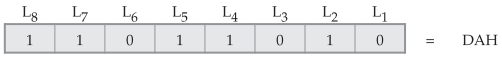
The
code (data) DAH must be sent on the latch to glow LEDs L1, L3
and L6.
Program
:
MVI
A, DAH ; Loads the data in the accumulator.
OUT
81H ; sends the data on the latch.
The
Fig. 7.2.4 shows the combined circuit for I/O interfacing. For this circuit the
address of input port is 80H and address of output port is 81H. The following
program displays the status of switches on the LEDs.
Program
:
IN
80H ; Read status of all switches.
OUT
81H ; send status on the output port.
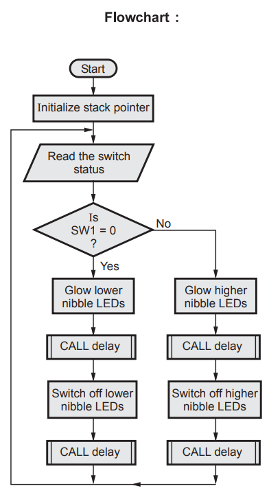
Example
7.2.1 Refer Fig. 7.2.4 and write a program that will
check the switch l status and do accordingly.
1.
SW1 = 0 : Blink lower nibble LEDs.
2.
SW1 = 1 : Blink higher nibble LEDs.
Assume
delay routine is available.
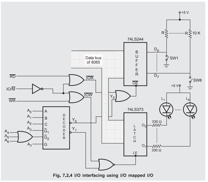
Solution
:
Input
port address = 80H
Output
port address = 81H
Source
Program :
LXI
SP, 27FFH ; Initialize stack
;
pointer
START
: IN 0H ; Read status of
;
switches
ANI
01H ; Masks Bit 1 to Bit 7
JNZ
HIGHER ; If swl status is
;
not zero goto
;
blink higher nibble
MVI
A, F0H ; Load bit
;
pattern to glow
;
lower nibble LEDs
OUT
81H ; Send it to
;
output port
CALL
Delay ; Call delay
;
subroutine
MVI
A, FFH ; Load bit pattern to switch off all LEDs
OUT
81H ; Send it to output
;
port
CALL
Delay ; Call delay
;
subroutine
JMP
START ; JUMP to START
HIGHER
: MVI A 0FH ; Load bit pattern to
;
glow higher
;
nibble LEDs
OUT
81H ; Send it to output port
CALL
Delay ; Call delay subroutine
OUT
81H ; Send it to output port
CALL
Delay ; Call delay subroutine
JUMP
START ; JUMP to START
Flowchart
:
4. Memory Mapped I/O
In
memory mapped I/O, the I/O devices are assigned and identified by 16-bit
addresses. The memory related instructions transfer the data between an I/O
device and the microprocessor, as long as I/O port is assigned to the memory
address space rather than to the I/O address space. The register associated
with the I/O port is simply treated as a memory location. Thus I/O device becomes
a part of the system's memory map and hence its name. In memory-mapped I/O
every instruction that refers to a memory location can control I/O. The source
and destination of the data is limited with I/O mapped I/O, since for an IN
instruction the destination register is always the accumulator and for the OUT
instruction the source register is always the accumulator. However, for memory
mapped I/O there are number of sources and destinations.
Instructions Interpretation for memory mapped I/O
Interpretation for memory mapped I/O
MOV
r, M ; Input from a port to specified register.
LDA
addr ; Input from a port to accumulator.
LHLD
addr ; Input from two ports to HL register pair.
ADD
M ; Port contents are added into accumulator
;
contents and result is stored in the accumulator.
ANA
M ; Port contents are logically ANDed with the accumulator
;
contents and result is stored in the accumulator.
ORA
M ; Port contents are logically ORed with the accumulator
;
contents and result is stored in the accumulator.
XRA
M ; Port contents are logically XORed with the accumulator
;
contents and result is stored in the accumulator.
CMP
M ; Compares the port contents with the accumulator
;
contents and updates the flag register contents accordingly.
MOV
M, r ; Outputs specified register contents to the port.
STA
addr MVI; Outputs accumulator contents to the port.
SHLD
addr ; Outputs HL register contents to two ports.
M,
data ; Outputs immediate data to the port.
Interfacing
of I/O port with memory mapped I/O
In
memory mapped I/O,  (memory read) and
  (memory write) control
signals are required to control the data transfer between I/O device and
microprocessor. As 8085 gives 16-bit memory address, it is necessary to decode
16-bit memory address to generate device select signal in case of memory mapped
1/O. Fig. 7.2.5 shows the interfacing of I/O devices in memory mapped I/O mode.
(memory write) control
signals are required to control the data transfer between I/O device and
microprocessor. As 8085 gives 16-bit memory address, it is necessary to decode
16-bit memory address to generate device select signal in case of memory mapped
1/O. Fig. 7.2.5 shows the interfacing of I/O devices in memory mapped I/O mode.

Example
7.2.2 Identify the port address and the mapping scheme
for the Fig. 7.2.6 given below.

Solution
:
Mapping scheme : I/O mapped I/O
a.
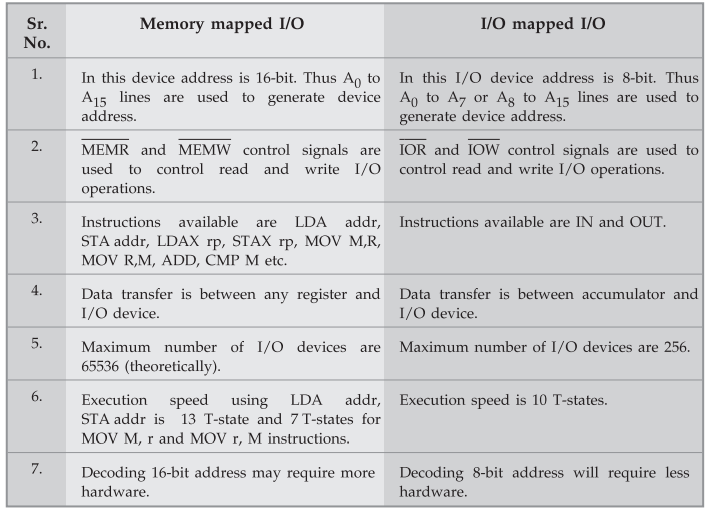
Comparison between Memory Mapped I/O and I/O Mapped I/O in 8085
Review Questions
1. With suitable
examples explain how I/O devices are connected using memory mapped I/O and
peripheral I/O.
2. Describe the
comparision qf I/O mapped and memory mapped I/O interfacing.
AU : May-04,12, Marks
8
3. Distinguish
peripheral mapped I/O and memory mapped I/O technique.
AU : May-07, Dec.-09,
Marks 8
4. Show the common
anode seven segment LED configuration. How to switch it on and off ?
AU : May-04, Marks 2
5. State the
disadvantages of memory mapped I/O scheme.
6. Write the
difference between memory mapped I/O and peripheral mapped I/O.
AU : Dec.-04,10;
May-06, Marks 2
7. Draw the decode
logic for LED output port in an I/O interface.
8. Compare memory
mapping and I/O mapping technique in 8085.
Microprocessors and Microcontrollers: Unit I: (e) I/O Interfacing : Tag: : - I/O Interfacing Techniques in 8085