Electron Devices and Circuits: Unit II: (d) UJT Thyristor and IGBT
IGBT
Construction, Principle of Operation, Symbols, Characteristics, Merits, Demerits, Applications
• The Insulated Gate Bipolar Transistor (IGBT) is the latest device in power electronics. It is obtained by combining the properties of BJT and MOSFET. We know that BJT has lower on-state losses for high values of collector current.
IGBT
AU
: May-16, 17
•
The Insulated Gate Bipolar Transistor (IGBT) is the latest device in power
electronics. It is obtained by combining the properties of BJT and MOSFET. We
know that BJT has lower on-state losses for high values of collector current.
But the drive requirement of BJT is little complicated. The drive of MOSFET is
very simple (i.e. only voltage is to be applied between gate and source). But
MOSFET has high on-state losses. The gate circuit of MOSFET and collector
emitter circuits of BJT are combined together to form a new device. This device
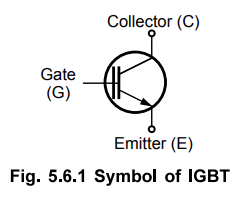
is called IGBT. Thus IGBT has advantages of both the BJT and MOSFETs. Fig.
5.6.1 shows the symbol of IGBT. Observe that the symbol clearly indicates
combination of MOSFET and BJT.
•
The IGBT has three terminals : Gate (G), collector (C) and emitter (E). Current
flows from collector to emitter whenever a voltage between gate and emitter is
applied. The IGBT is said to have turned 'on'. When gate emitter voltage is
removed, IGBT tums-off. Thus gate has full control over the conduction of IGBT.
When the gate to emitter voltage is applied, very small (negligible) current
flows. This is similar to the gate circuit of MOSFET. The on-state collector to
emitter drop is very small like BJT.
1. Construction of IGBT
•
The structure of IGBT is similar to that of MOSFET. Fig. 5.6.2 shows the
vertical cross-section of IGBT. In this structure observe that there is
additional p+ layer. This layer is collector (Drain) of IGBT.
•
This p+ injecting layer is heavily doped. It has the doping intensity of
1019per cm3. The doping of other layers is similar to that of MOSFET. n +
layers have 1019 per cm3, p-type body region has doping level of 1016 per cm3.
The n“ drift region is lightly doped (1014 per cm3).
a.
Punch through IGBT
•
The n+ buffer layer is not necessary for the operation of IGBT. The IGBTs which
have n+ buffer layer are called punch through IGBTs. Such IGBTs have asymmetric
voltage blocking capabilities. Punch through IGBTs have faster turn-off times.
Hence they are used for inverter and chopper circuits.
b.
Non-punch through IGBT
•
The IGBTs without n+ buffer layer are called non-punch through IGBTs. These
IGBTs have symmetric voltage blocking capabilities. These IGBTs are used for
rectifier type applications.
c.
Operation of IGBT
Similarity
of Operation with MOSFET
•
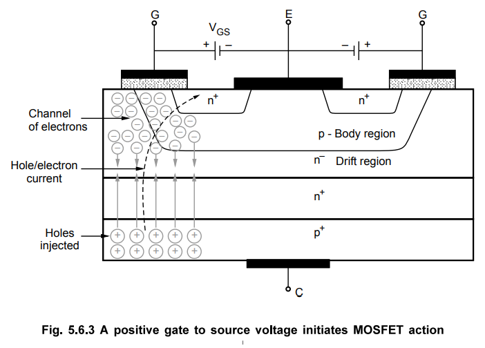
Now let us see how IGBT operates. When VGS > VGS(threshold)' channel of electrons is formed beneath
the gate as shown in Fig. 5.6.3. These electrons attract holes from p+ layer.
Hence, holes are injected from p+ layer into n_ drift region. Thus
hole/electron current starts flowing from collector to emitter. When holes
enter p-type body region, they attract more electrons from n+ layer. Ibis
action is exactly similar to MOSFET.
Difference
in operation Compared to MOSFET - Conductivity Modulation
•
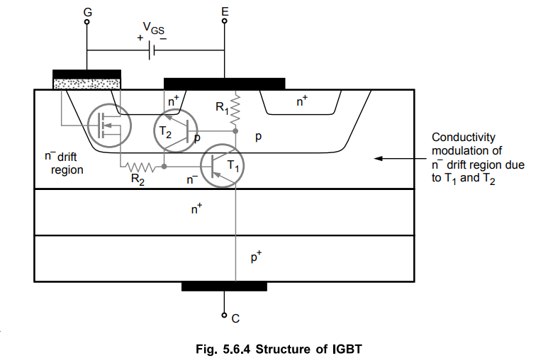
Now let us see how p+ injecting layer makes the operation different than
MOSFET. Fig. 5.6.4 shows the structure of IGBT showing how internal MOSFETs and
transistors are formed. The MOSFET is formed with input gate, emitter as source
and n “ drift region as drain. The two transistors Tx and T2 are formed as
shown. The holes injected by the p+ injecting layer go to the n “ drift region.
Ibis n_ drift region is base of Tx and collector of T2. The holes in the n “
drift region further go to the p-type body region, which is connected to the emitter.
The electrons from n + region (which is emitter) pass through the transistor Tj
and further in the n “ drift region. Thus holes and electrons are injected in
large amounts in n “ drift region. Ibis reduces the resistance of the n “ drift
region. This is called conductivity modulation of n “ drift region. Note that
such conductivity modulation does not exist in MOSFET.
How
on-state loss is reduced ?
•
The connection of Tx and T2 is such that large amount of hole/electrons are
injected in n “ drift region. The action of Tx and T2 is like SCR which is
regenerative. The gate serves as trigger for Tx through internally formed
MOSFET. Fig. 5.6.5 shows the equivalent circuit.
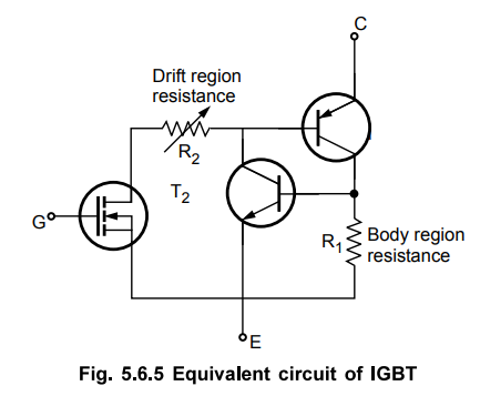
In
this Fig. 5.6.5 observe that when gate is applied (VGS > VGS(th)), the
internal equivalent MOSFET turns on. This gives base drive to Tx. Hence Tx
starts conducting. The collector of Tx is base of T^. Therefore T2 also turns
on. The collector of T2 is base of Tx. Thus the regenerative loop begins and
large number of carriers are injected in n “ drift region. This reduces the
on-state loss of the IGBT just like BJT. This happens due to conductivity
modulation of n “ drift region.
•
When the gate drive is removed, the IGBT should turn-off. When gate is removed,
the induced channel will be vanished and internal equivalent MOSFET will
turn-off. Hence Tx will turn-off if T2 tums-off. T2 will turn-off if the p-type
body region resistance Rx is very very small. Under such situation, its base
and emitter will be virtually shorted. Hence T2 turns-off. Therefore Tx will
also turn-off. Hence structure of IGBT is organized such that body region
resistance (Rx) is very very small.
•
If R1 is very very small, then T2 will never conduct and the equivalent circuit
of IGBT will be as shown in Fig. 5.6.6.
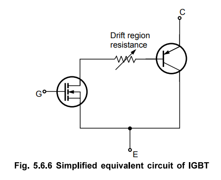
IGBTs
are thus different than MOSFETs because of conduction of current from collector
to emitter. For MOSFETs, on state losses are high since resistance of drift
region remains same. But in IGBTs, resistance of drift region reduces when gate
drive is applied. This resistance reduces because of p+ injecting region.
Hence, on-state loss of IGBT is very small.
d.
Latchup in IGBT
•
Latchup means IGBT remains in ON condition even if gate drive is removed.
•
Causes of latchup : The current in p-type body region flows vertically as well
as laterally. In equivalent circuit of Fig. 5.6.5 observe that the lateral
component of current flows through the body region resistance R-p Therefore the
drop across this body region resistance is sufficient to tum-on npn transistor
T2. Therefore pnp transistor T1 is also turned on and regeneration takes place.
Under this situation gate has no control over the current flow. Thus IGBT
remains in ON condition even if gate drive is removed.
•
To avoid latchups :
i)
Efforts are made to reduce the body resistance R1. This can be achieved by
using special geometries for the structure of IGBT.
ii)
The circuit should be designed in such a way that maximum specified current
should not be exceeded.
iii)
Latchups can also be avoided by increasing the turn-off time and controlling
hFE of the pnp transistor.
e.
Body-Source-Short and its Reason
What
is body-source-short ?
•
In the structure of IGBT observe that the source (or emitter 'E') is connected
to p-type body region as well as n+ region. This means p-type body region is
shorted to source (or emitter 'E').
Reason
• In Fig. 5.6.6 observe that various layers of
IGBT form internal parasitic thyristor i.e. (p+-n+n_ - p - n+). The
body-source-short avoids possible turn-on of this parasitic thyristor. The
base-emitter (i.e p-type body region and n+ region) of transistor T2 are
shorted due to body-source-short. Hence it does not conduct. It also helps in
avoiding latchup in IGBT.
2. Safe Operating Area (SOA) of IGBT
a.
Forward Biased SOA (FBSOA)
•
The FBSOA is the square for tum-on times less than 1 msec.
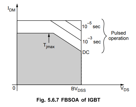
•
For reduced switching times FBSOA is limited by maximum junction temperature.
b.
Reverse Biased SOA (RBSOA)
•
The RBSOA depends upon the reapplied rate of change of drain-source voltage.
•
Observe that the RBSOA reduces as dVDs / dt increases.
•
The reduction in RBSOA is necessary to avoid latchups.
c.
Superiority ofSOA of IGBT and its Comparison with SOA of MOSFET and BJT
•
The SOA of IGBT is square for short switching times.
•
The RBSOA of IGBT indicates significantly higher values of reapplied dv/dt.
•
The SOA of IGBT is wider compared to that of BJT.
•
As switching frequency increases, the SOA of BJT reduces considerably.
•
The FBSOA of MOSFET and IGBT are similar for short switching times (i.e. less
than 1 ms).
•
The FBSOA of MOSFET and IGBT do not show second breakdown, since it is present
only in BJTs.
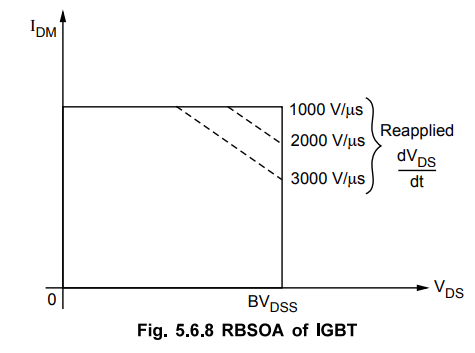
•
For longer switching times, the FBSOA of BJT, MOSFET and IGBT are restricted by
maximum junction temperature.
•
The RBSOA and FBSOA are identical in case of MOSFETs. But RBSOA is larger in
case of BJT and it is smaller in case of IGBT compared to their corresponding
FBSOA.
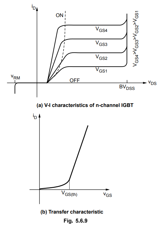
3. Steady State (V-l) and Transfer Characteristics of IGBT
a.
Steady State (V -1) or Output Characteristics
•
Fig. 5.6.9 (a) shows the V-I characteristics of n-channel IGBT. Sometime the
collector is also called drain and emitter is also called source. The
characteristics are plotted for drain (collector) current iD with respect to
drain source (collector emitter) voltage VDS. The characteristics are plotted
for different values of gate to source (VGS) voltages. When the gate to source
voltage is greater than the threshold voltage VGS (thy then IGBT turns-on. The
IGBT is off when VGS is less than VGS Fig. 5.6.9 shows the 'on' and 'off
regions of IGBT. The BVDSS is the breakdown drain to source voltage when gate
is open circuited. The IGBT is the popular device now-a-days. IGBT has simplest
drive circuit and it has low on-state losses.
(b)
Transfer characteristic
•
The drain current versus gate-source voltage is called transfer characteristic.
It is shown in Fig. 5.6.9 (b). This characteristic relates variation in output
current with respect to variation in input voltage. Transfer characteristics
are reasonably linear over most of the range of drain currents. The
characteristics becomes nonlinear when gate to source voltage approaches
VGS(th). When the gate to source voltage is less than VGS(th) i.e. threshold
value, the IGBT goes in off state.
4. Switching Characteristics of IGBT
•
Fig. 5.6.10 shows the switching characteristics of IGBT. The gate to source
voltage is normally negative. This voltage is made positive to tum-on the IGBT.
When VGS > VGS(th)' collector
current starts increasing. Tum-on delay, td(on) is the delay when gate drive is
applied and ic starts increasing. When ic increases to its full value,
collector emitter voltage starts falling. 'tri' is the rise time of collector
and tfv is the fall time of voltage. Thus, tum-on time of IGBT is,
ton
= td(on) + tri + tfv
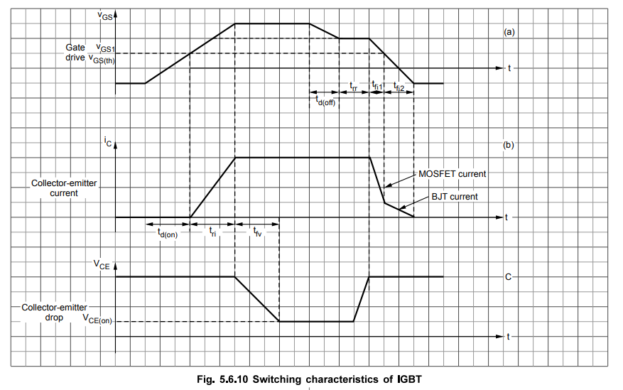
•
The turn-off of the IGBT is initiated by reducing the gate voltage. When gate
voltage falls to the value equal to vGS1, VCE starts
rising. VGS1 is the voltage where IGBT comes out of saturation.
Turn-off delay, td(off) is the delay time when gate voltage is reduced and VCE
starts increasing. When VCE reaches to supply voltage, ic starts reducing. ic
reduces fast till vGs reaches to vGS(th). This fast decay in ic is basically
due to internal MOSFET. Then VGS goes to zero and becomes negative. But ic
keeps on flowing for sometime. This is internal BJT current. This current flows
due to stored carriers in the drift region. Hence, turn-off time of IGBT is
higher than IGBT. The turn-off time of IGBT will be,
toff
= td(off) + trv + tfi1 + tfi2
Here, trv is voltage rise time.
tfi1
is MOSFET current fall
time.
tfi2
is BJT current fall time.
5. Merits, Demerits and Applications of IGBT
a.
Merits of IGBT
i)
Voltage controlled device. Hence drive circuit is very simple.
ii)
On-state losses are reduced compared to BJT, MOSFET and SCR.
iii)
Switching frequencies are higher than thyristors.
iv)
No commutation circuits are required as compared to SCR.
v)
Gate have full control over the operation of IGBT.
vi)
IGBTs have approximately flat temperature coefficient.
vii)
The drive of IGBT is simple and driving current requirement is also very small
as compared to BJT, since there is no direct current flow in the gate.
viii)
The voltage and current ratings of the IGBTs are better compared to MOSFETs.
b.
Demerits of IGBT
i)
IGBTs have static charge problems.
ii)
IGBTs are costlier than BJTs and MOSFETs.
c.
Applications of IGBTs
i)
AC motor drives, i.e. inverters.
ii)
DC to DC power supplies, i.e choppers.
iii)
UPS systems.
iv)
Harmonic compensators.
Review Questions
1. Explain the
construction and characteristics of IGBT.
2. Explain the
construction and operation of IGBT with neat diagrams.
3. Explain the
characteristics of IGBT.
4. State the merits,
demerits and applications of IGBT.
Electron Devices and Circuits: Unit II: (d) UJT Thyristor and IGBT : Tag: : Construction, Principle of Operation, Symbols, Characteristics, Merits, Demerits, Applications - IGBT
Related Topics
Related Subjects

Electron Devices and Circuits
EC3301 3rd Semester EEE Dept | 2021 Regulation | 3rd Semester EEE Dept 2021 Regulation