Microprocessors and Microcontrollers: Unit III: (a) 8051 Microcontroller
Interfacing and Timing Diagrams for Memory Interfacing
8051 Microcontroller
We have seen that 8051 has internal data and code memory with limited memory capacity. This memory capacity may not be sufficient for some applications.
Interfacing and Timing Diagrams for Memory Interfacing
AU
: Dec.-10, 17, 18, May-12
We
have seen that 8051 has internal data and code memory with limited memory
capacity. This memory capacity may not be sufficient for some applications. In
such situations, we have to connect external ROM/EPROM and RAM to 8051
microcontroller to increase the memory capacity. We also know that ROM is used
as a program memory and RAM is used as a data memory. Let us see how 8051
accesses these memories.
1. External Program Memory
Fig.
14.6.1 shows a map of the 8051 program memory

In
8051, when the ![]() pin is connected to VCC, program fetches to
addresses 0000H through 0FFFH are directed to the internal ROM and program
fetches to addresses 1000H through FFFFH are directed to external ROM/EPROM. On
the other hand when
pin is connected to VCC, program fetches to
addresses 0000H through 0FFFH are directed to the internal ROM and program
fetches to addresses 1000H through FFFFH are directed to external ROM/EPROM. On
the other hand when ![]() pin is grounded, all addresses (0000H to FFFFH) fetched by program are directed
to the external ROM/EPROM. The
pin is grounded, all addresses (0000H to FFFFH) fetched by program are directed
to the external ROM/EPROM. The  signal is used to activate output enable
signal of the external ROM/EPROM, as shown in the Fig. 14.6.2.
signal is used to activate output enable
signal of the external ROM/EPROM, as shown in the Fig. 14.6.2.

As
shown in the Fig. 14.6.2, the port 0 is used as a multiplexed address/bus. It
gives lower order 8-bit address in the initial T-cycle and later it is used as
a data bus. The 8-bit address is latched using external latch and ALE signal
generated by 8051. The port 2 provides the higher order 8-bit address. Fig. 14.6.3
shows the timing waveforms for external program memory read cycle.

The
lower part of program memory stores the vector addresses for various interrupt
service routines. Fig. 14.6.4 shows the vector address map. Each interrupt is
assigned with a fixed location in program memory. For example, external
interrupt 0 is assigned to location 0003H. The interrupt service locations are
spaced at 8-byte intervals such as 0003H for External Interrupt 0, 000BH for
Timer 0, 0013H for External Interrupt 1, 001BH for Timer 1, etc. If interrupt
is going to be used, its service routine must begin at corresponding location. If the interrupt
is not going to be used, its service location is available as general purpose
program memory.

Instructions
to Access External ROM / Program Memory
The
Table 14.6.1 explains the instructions to access external ROM/program memory.

2. External Data Memory
Fig.
14.6.5 shows a map of the 8051 data memory.

The 8051 can address upto 64 kbytes of external data memory. The "MOVX" instruction is used to access the external data memory. The internal data memory space for 8051 is divided into three blocks : Lower 128 bytes, Upper 128 bytes and SFRs. The upper addresses and SFRs occupy the same block of address space, 80H through FFH, although they are physically separate entities. As shown in the Fig. 14.6.5, the upper address space is accessible by indirect addressing only and SFRs are accessible by direct addressing only. On the other hand, lower address space can be accessed either by direct addressing or by indirect addressing.
Fig.
14.6.6 shows the circuit diagram for
connecting external data memory. The multiplexed address/data bus provided by
port 0 is demultiplexed by external latch and ALE signal. Port 2 gives the
higher order address bus. The 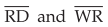 signals from 8051 selects the memory
read and memory write operation, respectively.
signals from 8051 selects the memory
read and memory write operation, respectively.

Fig.
14.6.7 (a) and (b) shows the timing
waveforms for external data memory read and write cycles, respectively.

Instructions
to Access External Data Memory
The
Table 14.6.2 explains the instruction to access external data memory.

3. Important Points to Remember in Accessing External Memory
•
All external data moves with external ROM or external RAM involve the A
register.
•
While accessing external memory, Rp can address 256 bytes and DPTR can address
64 kbytes.
•
MOVX instruction is used to access external RAM or I/O addresses.
When
PC is used to access external ROM, it is incremented by 1 (to point to the next
instruction) before it is added to A to form the physical address of external
ROM.
Example
14.6.1 An 8051 based system requires external memory of
four 4 kbytes of SRAM each and two chips of EPROM of size 2 kbytes. The EPROM
starts at address 2000H. SRAM address map follows EPROM map. Give the complete
interface.
Solution
:

Example
15.6.2 Interface two 8255's to 8051 with stating
address of OF000H. Show the hardware design. Write the instruction sequence to
initialize all ports of first 8255 as output ports in mode 0 and in the second
8255 port A as input in mode 1 and other ports as input in mode 0.

Address Map :

For
8255 (0) first :
MOV
A, # 80H ; Load control word
MOV
DPTR, # OF003H ; Initialize DPTR with address of CR
MOVX@DPTR,
A ; Send the control word
For
8255 (1) second :
MOV
A, # BBH ; Load control word
MOV
DPTR, # OF007H ; Initialize DPTR with address of CR
MOVX
@ DPTR, A ; Send the control word
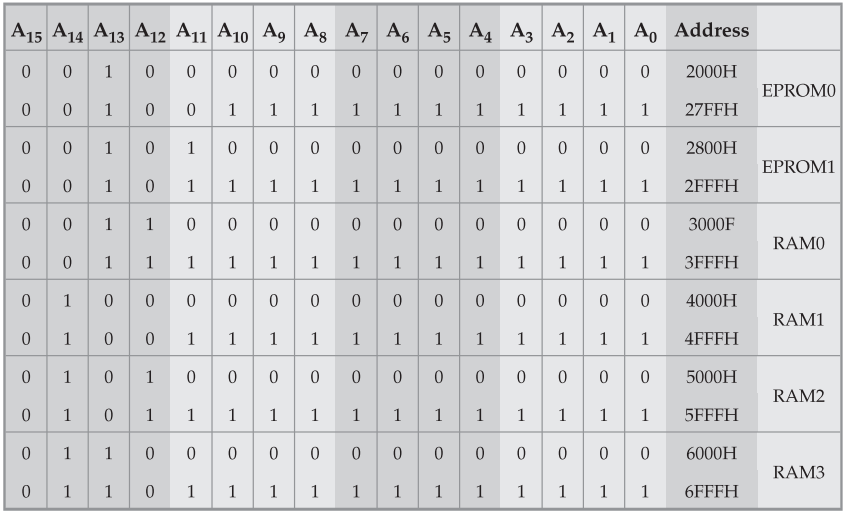
Example
14.6.2 Give the complete block schematic of an 8051 based
system having following specifications.
64
kB of program memory.
64
kB of data memory.
Make
use of 16 K × 8-bit memory chips and 74 LS 138 decoders.
Indicate
clearly, the addresses selected for the memory chips.
Solution
:
See
Fig. 14.6.10

Memory
Map :
Review Questions
1. Explain program
memory interfacing in 8051 microcontroller.
2. Design an 8051
based system with 16 kbytes qf program ROM and 16 kbytes of data ROM.
AU : Dec.-10, Marks 16
3. Explain in detail
the different methods of memory address decoding in 8051.
AU : Dec.-10, Marks 8
4. Explain with block
diagram, how to access external memory devices in an 8051 based system.
AU : Dec.-17, Marks 6
5. Describe the timing
diagram of external data memory read cycle of 8051.
AU : Dec.-18, Marks 13
Microprocessors and Microcontrollers: Unit III: (a) 8051 Microcontroller : Tag: : 8051 Microcontroller - Interfacing and Timing Diagrams for Memory Interfacing