Microprocessors and Microcontrollers: Unit IV: (f) A/D and D/A Converter Interfacing with 8085
Interfacing of ADC 0808 with 8085
A/D and D/A Converter Interfacing with 8085
ADC 0808 has eight input channels, so to select desired input channel, it is necessary to send 3-bit address on ADC, ADB and ADA inputs.
Interfacing of ADC 0808 with 8085
Fig.
13.6.1 shows interfacing of ADC 0808 with 8085 using 8255. ADC 0808 has eight
input channels, so to select desired input channel, it is necessary to send
3-bit address on ADC, ADB and ADA inputs. The address of the desired channel is
sent to the multiplexer address inputs through PB0 to PB2
lines.

After
at least 50 ns, this address must be latched. This is achieved by sending ALE
signal using port line PB3. After another 2.5 ,us the start of conversion
signal (SOC) must be sent high and then low. Port line PB4 is used for this
purpose. The end of conversion (EOC) is detected by port line PC0. The Fig. 13.6.2
shows timing waveforms for the ADC 0808. Schmitt-trigger inverter circuitry
generates 300 kHz clock which is required to operate ADC 0808. The zener diode
and LM 308 amplifier circuitry is used to produce a VCC and and + VREF
of 5.12 V for the A/D converter. With this reference voltage the A/D converter
will have 256 steps of 20 mV each. (See Fig. 13.6.2 )

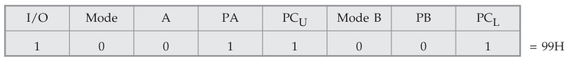
I/O Map

Control Word
Routine
does the conversion and reads the digital data
MVI
A, 99H ; initialize 8255
OUT
CR
MVI
A, 00H
OUT
PB ; Send address to select channel 0
MVI
A, 08H
OUT
PB ; Latch the given address by sending ALE high
Call
Delay ; Wait for at least 2.5 µs
MVI
A, 18H
OUT
PB ; Make SOC high
NOP ; Wait for at least 05 µs
MVI
A, 08H
OUT
PB ; Make SOC low
CHECK
: IN PC ; Check for EOC
ANI
01
JZ
CHECK ; If no, repeat
IN
PA ; Read digital input
RET
; Return
Review Questions
1. Explain the
interfacing of A/D converter with microprocessor.
2. Interface a ADC
chip with 8085 processor through 8255 ports and write and ALP to use BSR mode
to START conversion and STATUS CHECK mode to read output data. Explain the
complete circuit and programs. Use I/O mapped I/O configuration. AU : May-04, Marks 16
3. With neat diagram
explain the ADC interface to microprocessor.
AU : Dec.-04,10,11,
May-08,11, Marks 16
4. Using peripheral mapped I/O, design an interface circuit to connect an ADC 0808 to a microprocessor. AU : May-05, Marks 6
5. Explain how 8085
can be connected to an A/D convertor. Describe the signals involved in the
process of conversion.
AU: Dec.-05, Marks
12
6. What are the
steps involved in interfacing an ADC with 8085.
AU : Dec.-09, Marks
4
7. Show and explain
the ADC interfacing with 8085 microprocessor.
AU May-11, Marks 8
8. Why do we need
A/D converter and D/A converter? Draw the block diagram to interface 8085
microprocessor with A/D convertor and D/A convertor.
AU: Dec.-11, Marks 8
9. Draw and describe
the interfacing of A/D and D/A converter interfacing to 8085 microprocessor.
AU: May-12, Marks 8
Microprocessors and Microcontrollers: Unit IV: (f) A/D and D/A Converter Interfacing with 8085 : Tag: : A/D and D/A Converter Interfacing with 8085 - Interfacing of ADC 0808 with 8085