Microprocessors and Microcontrollers: Unit III: (a) 8051 Microcontroller
Internal and External Memories
The 8051 has 4 K bytes of internal program memory and 256 bytes of internal data memory.
Internal and External Memories
Fig.
14.5.1 shows the basic memory structure for 8051. It can access up to 64 K
program memory and 64 K data memory. The 8051 has 4 K bytes of internal program
memory and 256 bytes of internal data memory.

1. Internal RAM Organization
The
8051 has 128-byte internal RAM. It is accessed using RAM address register. The
Fig. 14.5.2 shows the organization of internal RAM. As shown in the Fig. 14.5.2
internal RAM of 8051 is organized into three distinct areas :
•
Register bank
•
Bit addressable
•
General purpose.
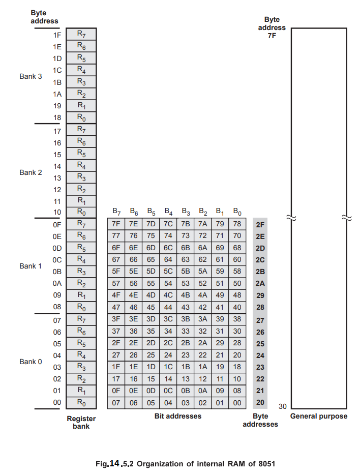
a.
8051 Register Banks (Working Registers)
The
first 32-bytes from address OOH to 1FH of internal RAM constitute 32 working
registers. They are organized into four banks of eight registers each. The four
register banks are numbered 0 to 3 and are consists of eight registers named R0
to R7.
Each
register can be addressed by name or by its RAM address.
Only
one register bank is in use at a time. Bits RSO and RSI in the PSW determine
which bank of registers is currently in use.
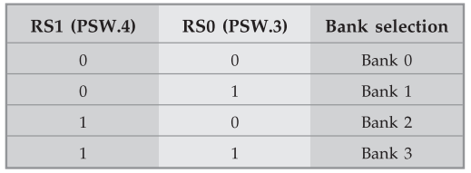
On
reset, the bank 0 is selected and hence it is a default register bank. Register
banks when not selected can be used as general purpose RAM.
b. Bit / Byte Addressable
The
8051 provides 16 bytes of a bit-addressable area. It occupies RAM byte
addresses from 20H to 2FH, forming a total of 128 (16 × 8) addressable bits.
An
addressable bit may be specified by its bit address of 00H to 7FH, or 8 bits
may form any byte address from 20H to 2FH.
For
example, bit address 4EH refers bit 6 of the byte address 29H.
c. General Purpose RAM
The
RAM area above bit addressable area from 30H to 7FH is called general purpose
RAM. It is addressable as byte.
2. ROM Space in the 8051
The
8051 has 4 kbyte of internal ROM with address space from 0000H to OFFFH. It is
programmed by manufacturer when the chip is built. This part cannot be erased
or altered after fabrication. This is used to store final version of the
program. It is accessed using program address register.
Review Questions
1. What do you
understand by bit addressable RAM in 8051 microcontroller ? AU : Dec.-10
2. Discuss the
internal memory organization of the 8051 microcontroller. AU : Dec.-10, May-11,
Marks 16
3. Discuss about the
organization of internal RAM and special function registers of 8051 microcontroller
in detail.
4. Discuss in datail
internal data memory organization of microcontroller 8051. AU : Dec.-19, Marks 8
5. Explain the program
memory and data memory structure of 8051 microcontroller. AU : Dec.-11, Marks 8
7. Explain the RAM structure of 8051 microcontroller.
Microprocessors and Microcontrollers: Unit III: (a) 8051 Microcontroller : Tag: : - Internal and External Memories