Microprocessors and Microcontrollers: Unit V: (b) Introduction to RISC Based Architecture
Interrupts and its Programming
• The PIC18 devices have multiple interrupt sources depending on which peripherals are incorporated in the chip. Some of the most widely used interrupt sources of PIC18 are : ■ External hardware interrupts : INTO, INT1 and INT2 ■ Timer interrupts : TMROIF, TMR11F, TMR2IF and TMR3IF ■ Serial communication interrupts : TXIF and RCIF ■ RB Port change interrupt: RBIF ■ A/D converter interrupt: ADIF ■ Compare, capture, PWM interrupt: CCP1IF
Interrupts and its Programming
•
The PIC18 devices have multiple interrupt sources depending on which
peripherals are incorporated in the chip. Some of the most widely used
interrupt sources of PIC18 are :
■
External
hardware interrupts : INTO, INT1 and INT2
■
Timer
interrupts : TMROIF, TMR11F, TMR2IF and TMR3IF
■
Serial
communication interrupts : TXIF and RCIF
■
RB
Port change interrupt: RBIF
■
A/D converter interrupt: ADIF
■
Compare,
capture, PWM interrupt: CCP1IF
•
Fig. 18.16.1 shows the simplified interrupt structure of PIC18.

•
Each interrupt source has three bits to control its operation. The functions of
these bits are:
■
Flag
bit to indicate that an interrupt event occurred.
■
Enable
bit that allows program execution to branch to the interrupt vector address
when the flag bit is set.
■
Priority
bit to select high priority or low priority.
1. Enabling and Disabling Interrupts
When
PIC18 is reset, all interrupts are disabled. These are enabled by software. All
of the bits that generate interrupts can be set or cleared by software.
•
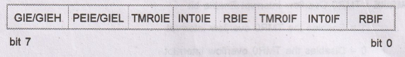
Fig. 18.16.2 shows the bit pattern for the INTCON register.

bit
7 : Global Interrupt Enable bit
1
= Enables all unmasked interrupts
0
= Disables all interrupts
bit
6 PEIE : Peripheral Interrupt Enable bit
1
= Enables all unmasked peripheral interrupts
0
= Disables all peripheral interrupts
bit
5 TMR0IE: TMR0 Overflow Interrupt Enable bit
1
= Enables the TMR0 overflow interrupt
0
= Disables the TMR0 overflow interrupt
bit
4 INT0IE: INT0 External Interrupt Enable
bit
1
= Enables the INT0 external interrupt
0
= Disables the INT0 external interrupt
Bit
3 RBIE : RB Port Change Interrupt Enable bit
1
= Enables the RB port change interrupt
0
= Disables the RB port change interrupt
Fig.
18.16.2 Bit pattern for the INTCON register
•
The PEIE bit (INTCON register) enables/disables all peripheral interrupt
sources. The GIE bit (INTCON register) enables/disables all interrupt sources.
Steps
in Enabling Interrupt
1.
Make GIE bit (INTCON register: Bit 7) = 1 to enable all maskable interrupts.
2.
Set the dedicated interrupt enable flag bit for the interrupt to be used.
3.
If we want to use peripheral interrupts, enable them by making PEIE (Peripheral
Interrupt Enable bit) of INTCON register high.
2. Interrupt Registers
•
For the PIC18F458 microcontroller, 13 registers are used to control interrupt
operation. These registers are :
■
RCON
■
INTCON
■
INTCON2
■
INTCON3
■
PIR1,
PIR2, PIR3
■
PIE1,
PIE2, PIE3
■
IPR1,
IPR2, IPR3-
a.
INTCON Registers
•
The INTCON registers are readable and writable registers that contain various
enable, priority and flag bits. Because of the number of interrupts to be
controlled, PIC18FXX8 devices have three INTCON registers.
INTCON
Register
bit
7 GIE/GIEH: Global Interrupt Enable bit
When
IPEN (RCON < 7) = 0;
1
= Enables all unmasked interrupts
0
= Disables all interrupts
When
IPEN (RCON <7>) = 1;
1
= Enables all high priority interrupts
0
= Disables all priority interrupts
bit
6 PEIE/GIEL: Peripheral Interrupt Enable bit
When
IPEN (RCON < 7 >) = 0;
1
Enables all unmasked peripheral interrupts
0
= Disables all peripheral interrupts
When
IPEN (RCON <7>) = 1;
1
= Enables all low priority peripheral interrupts
0
= Disables all low priority peripheral interrupts
bit
5 TMR0IE : TMR0 Overflow Interrupt Enable bit
1
= Enables the TMR0 overflow interrupt
0
= Disables the TMR0 overflow interrupt
bit
4 INT0IE: INT0 External Interrupt Enable bit
1
= Enables the INT0 external interrupt
0
= Disables the INT0 external interrupt
bit
3 RBIE: RB Port Change Interrupt Enable bit
1
= Enables the RB port change interrupt
0
= Disables the RB port change interrupt
bit
2 TMR0IF: TMR0 Overflow Interrupt Flag bit
1
= TMR0 register has overflowed (must be cleared in software)
0
= TMR0 register did not overflow
bit
1 INT0IF : INT0 External Interrupt Flag bit
1
= The INT0 external interrupt occurred (must be cleared in software by reading
PORTB)
0
= The INTO external interrupt did not occur
bit
0 RBIF: RB Port Change Interrupt Flag bit
1
= At least one of the RB7 : RB4 pins changed state (must be cleared in
software)
0
= None of the RB7 RB4 pins have changed state
Fig.
18.16.3 Bit pattern for INTCON register
INTCON2
Register

1
= All PORTB pull-ups are disabled
0
= PORTB pull-ups are enabled by individual port latch values
bit
6 INTEDG0: External Interrupt 0 Edge Select bit
1
= Interrupt on rising edge
0
= Interrupt on falling edge
bit
5 INTEDG1: External Interrupt 1 Edge Select bit
1
= Interrupt on rising edge
0
= Interrupt on falling edge
bit
4-3 Unimplemented: Read as '0'
bit
2 TMR0IP: TMR0 Overflow Interrupt Priority bit
1
= High priority
2
= Low priority
bit
1 RBIP: RB Port Change Interrupt Priority bit
1
= High priority
0
= Low priority
Fig.
18.16.4 Bit pattern for INTCON2 register
INTCON3
Register
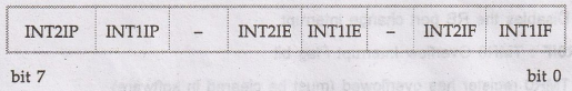
bit
7 INT2IP : INT2 External Interrupt Priority bit
1
= High priority
0
= Low priority
bit
6 INT1IP : INT1 External Interrupt Priority bit
1
= High priority
0
= Low priority
bit
5 Unimplemented : Read as '0'
bit
4 INT2IE : INT2 External Interrupt Enable bit
1
= Enables the INT2 external interrupt
0
= Disables the INT2 external interrupt
bit
3 INT1IE : INT1 External Interrupt Enable bit
1
= Enables the INT1 external interrupt
0
= Disables the INT1 external interrupt
bit
2 Unimplemented : Read as '0'
bit
1 INT2IF : INT2 External Interrupt Flag bit
1
= The INT2 external interrupt occurred (must be cleared in software)
0
= The INT2 external interrupt did not occur
bit
0 INT1IF : INT1 External Interrupt Flag bit
1
= The INT1 external interrupt occurred (must be cleared in software)
0
= The INT1 external interrupt did not occur
Fig.
18.16.5 Bit pattern for INTCON3 register
b.
PIR Registers
•
The Peripheral Interrupt Request (PIR) registers contain the individual flag
bits for the peripheral interrupts.
•
Due to the number of peripheral interrupt sources, there are three Peripheral
Interrupt Request (Flag) registers (PIR1, PIR2, PIR3).
PIR1:
Peripheral Interrupt Request (Flag) Register 1
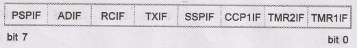
bit
7 PSPIF: Parallel Slave Port Read/Write Interrupt Flag bit
1
= A read or a write operation has taken place (must be cleared in software)
0
= No read or write has occurred
bit
6 ADIF: A/D Converter Interrupt Flag bit
1
= An A/D conversion completed (must be cleared in software)
0
= The A/D conversion is not complete
bit
5 RCIF: USART Receive Interrupt Flag bit
1
= The USART receive buffer, RCREG is full (cleared when RCREG is read)
0
= The USART receive buffer is empty
bit
4 TXIF : USART Transmit Interrupt Flag bit
1
= The USART transmit buffer, TXREG is empty (cleared when TXREG is written)
0
= The USART transmit buffer is full
bit
3 SPPIF: Master Synchronous Serial Port Interrupt Flag bit
1
= The transmission/reception is complete (must be cleared in software)
0
= Waiting to transmit/receive
bit
2 CCP1IF : CCP1 Interrupt Flag bit
Capture
mode :
1
= A TMR1 register capture occurred (must be cleared in software)
0
= No TMR1 register capture occurred
Compare
mode :
1
= A TMR1 register compare match occurred (must be cleared in software)
0
= No TMR1 register compare match occurred
PWM
mode :
Unused
in this mode.
bit
1 TMR2IF : TMR2 to PR2 Match Interrupt Flag bit
1
= TMR2 to PR2 match occurred (must be cleared in software)
0
= No TMR2 to PR2 match occurred
bit
0 TMR1IF: TMR1 Overflow Interrupt Flag bit
1=
TMR1 register overflowed (must be cleared in software)
0
= TMR1 register did not overflow
Fig.
18.16.6 Bit pattern for Peripheral Interrupt Request (Flag) Register 1
PIR2:
Peripheral Interrupt Request (Flag) Register 2
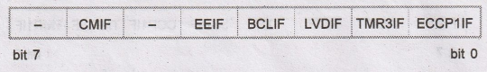
bit
7 Unimplemented : Read as '0'
bit
6 CMIF: Comparator Interrupt Flag bit
1
= Comparator input has changed
0
= Comparator input has not changed
bit
5 Unimplemented : Read as '0'
bit
4 EEIF : EEPROM Write Operation Interrupt Flag bit
1
= Write operation is complete (must be cleared in software)
0
= Write operation is not complete
bit
3 BCLIF : Bus Collision Interrupt Flag bit
1
= A has collision occurred (must be cleared in software)
0
= No bus collision occurred
bit
2 LVDIF : Low-Voltage Detect Interrupt Flag bit
1
= A low-voltage condition occurred (must be cleared in software)
0
= The device voltage is above the Low-Voltage Detect trip point
bit
1 TMR3IF : TMR3 Overflow Interrupt Flat bit
1
= TMR3 register overflowed (must be cleared in software)
0
= TMR3 register did not overflow
bit
0 ECCP1IF: ECCP1 Interrupt Flag bit
Capture
mode :
1
= A TMR1 (TMR3) register capture occurred (Must be cleared in software)
0
= No TMR1 (TMR3) register capture occurred
PWM
mode :
Unused
in this mode.
Fig.
18.16.7 Bit pattern for Peripheral Interrupt Request (Flag) Register 2
PIR
3 : Peripheral Interrupt Request (Flag) Register 3

bit
7 IRXIF : Invalid Message Received Interrupt Flag bit
1
= An invalid message has occurred on the CAN bus
0
= An invalid message has not occurred on the CAN bus
bit
6 WAKIF : Bus Activity Wake-up Interrupt Flag bit
1
= Activity on the CAN bus has occurred
0
= Activity on the CAN bus has not occurred
bit
5 ERRIF : CAN bus Error Interrupt Flag bit
1
= An error has occurred in the CAN module (multiple sources)
0
= An error has not occurred in the CAN module
bit
4 TXB2IF : Transmit Buffer 2 Interrupt Flag bit
1
= Transmit Buffer 2 has completed transmission of a message and may be reloaded
0
= Transmit Buffer 2 has not completed transmission of a message
bit
3 TXB1IF : Transmit Buffer 1 Interrupt Flag bit
1
= Transmit Buffer 1 has completed transmission of a message and may be reloaded
0
= Transmit Buffer 1 has not completed transmission of a message
bit
2 TXB0IF : Transmit Buffer 0 Interrupt Flag bit
1
= Transmit Buffer 0 has completed transmission of a message and may be reloaded
0
= Transmit Buffer 0 has not completed transmission of a message
bit
1 RXB1IF : Receiver Buffer 1 Interrupt Flag bit
1
= Transmit Buffer 1 has completed transmission of a message and may be reloaded
0
= Transmit Buffer 1 has not completed transmission of a message
bit
0 TXB1IF : Receiver Buffer 0 Interrupt Flag bit
1
= Transmit Buffer O has completed transmission of a message and may be reloaded
0
= Transmit Buffer O has not completed transmission of a message
Fig.
18.16.8 Bit pattern for Peripheral Interrupt Request (Flag) Register 3
c.
PIE Registers
•
The Peripheral Interrupt Enable (PIE) registers contain the individual enable
bits for the peripheral interrupts.
•
Due to the number of peripheral interrupt sources, there are three Peripheral
Interrupt Enable registers (PIE1, PIE2, PIE3).
•
When IPEN is clear, the PEIE bit must be set to enable any of these peripheral
interrupts.
PIE1:
Peripheral Interrupt Enable Register 1

bit
7 PSPIE : Parallel Slave Port Read/Write Interrupt Enable bit
1
= Enables the PSP read/write interrupt
0
= Disables the PSP read/write interrupt
bit
6 ADIE : A/D Converter Interrupt Enable bit
1
= Enables the A/D interrupt
0
= Disables the A/D interrupt
bit
5 RCIE : USART Receive Interrupt Enable bit
1
= Enables the USART receiver interrupt
0
= Disables the USART receive interrupt
bit
4 TXIE : USART Transmit Interrupt Enable bit
1
= Enables the USART transmit interrupt
0
= Disables the USART transmit interrupt
bit
3 SSPIE : Master Synchronous Serial Port
Interrupt
Enable bit
1
= Enables the MSSP interrupt
0
= Disables the MSSP interrupt
bit
2 CCP1IE : CCP1 Interrupt Enable bit
1
= Enables the CCP1 interrupt
0
= Disables the CCP1 interrupt
bit
1 TMR2IE : TMR2 to PR2 Match Interrupt Enable bit
1
= Enables the TMR2 to PR2 match interrupt
0
= Disables the TMR2 to PR2 match interrupt
bit
0 TMR1IE : TMR1 Overflow Interrupt Enable bit
1
= Enables the TMR1 overflow interrupt
0
= Disables the TMR1 overflow interrupt
Fig.
18.16.9 Bit pattern for peripheral interrupt enable register 1
PIE2:
Peripheral Interrupt Enable Register 2
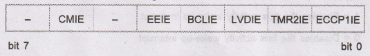
bit
7 Unimplemented : Read as '0'
bit
6 CMIE : Comparator Interrupt Enable bit
1
= Enables the comparator interrupt
0
= Disables the comparator interrupt
bit
5 Unimplemented : Read as '0'
bit
4 EEIE : EEPROM Write Interrupt Enable bit
1
= Enabled
0
= Disabled
bit
3 BCLIE : Bus Colliion Interrupt Enable bit
1
= Enabled
0
= Disabled
bit
2 LVDIE : Low-Voltage Detect Interrupt Enable bit
1
= Enabled
0
= Disabled
bit
1 TMR3IE : TMR3 Overflow Interrupt Enable bit
1
= Enables the TMR3 overflow interrupt
0
= Disables the TMR3 overflow interrupt
bit
0 ECCP1IE : ECCP1 Interrupt Enable bit
1
= Enables the ECCP1 interrupt
0
= Disables the ECCP1 interrupt
Fig.
18.16.10 Bit pattern for Peripheral Interrupt Enable Register 2
PIE3:
Peripheral Interrupt Enable Register 3d
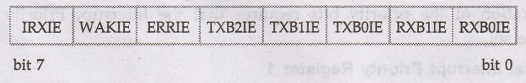
bit
7 IRXIE : Invalid CAN Message Received Interrupt Enable bit
1
= Enables the invalid CAN message received interrupt
0
= Disables the invalid CAN message received interrupt
bit
6 WAKIE : Bus Activity Wake-up Interrupt Enable bit
1
= Enables the bus activity wake-up interrupt
0
= Disables the bus activity wake-up interrupt
bit
5 ERRIE : CAN bus Error Interrupt Enable bit
1
= Enables the CAN bus error interrupt
0
= Disables the CAN bus error interrupt
bit
4 TXB2IE : Transmit Buffer 2 Interrupt Enable bit
1
= Enables the Transmit Buffer 2 interrupt
0
= Disables the Transmit Buffer 2 interrupt
bit
3 TXB1IE : Transmit Buffer 1 Interrupt Enable bit
1
= Enables the Transmit Buffer 1 interrupt
0
= Disables the Transmit Buffer 1 interrupt
bit
2 TXB0IE: Transmit Buffer 0 Interrupt Enable bit
1
= Enables the Transmit Buffer O interrupt
0
= Disables the Transmit Buffer 0 interrupt
bit
1 RXB1IE : Receive Buffer 1 Interrupt Enable bit
1
= Enables the Receive Buffer 1 interrupt
0
= Disables the Receive Buffer 1 interrupt
bit
0 RXBOIE : Receive Buffer 0 Interrupt Enable bit
1
= Enables the Receive Buffer 0 interrupt
0
= Disables the Receive Buffer 0 interrupt
Fig.
18.16.11 Bit pattern for Peripheral Interrupt Enable Register 3
d.
IPR Registers
•
The Interrupt Priority (IPR) registers contain the individual priority bits for
the peripheral interrupts. Due to the number of peripheral interrupt sources,
there are three Peripheral Interrupt Priority registers (IPR1, IPR2 and IPR3).
•
The operation of the priority bits requires that the Interrupt Priority Enable
bit (IPEN) be set.
IPR1:
Peripheral Interrupt Priority Register 1
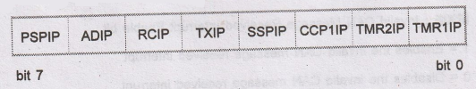
bit
7 PSPIP : Parallel Slave Port Read/Write Interrupt Priority bit
1
= High priority
0
= Low priority
bit
6 ADIP: A/D Converter Interrupt Priority bit
1
= High priority
0
= Low priority
bit
5 RCIP : USART Transmit Interrupt Priority bit
1
= High priority
0
= Low priority
bit
4 TXIP : USART Transmit Interrupt Priority bit
1
= High priority
0
= Low priority
bit
3 SSPIP : Master Synchronous Serial Port Interrupt Priority bit
1
= High priority
0
= Low priority
bit
2 CCP1IP : CCP1 Interrupt Priority bit
1
= High priority
0
= Low priority
bit
1 TMR2IP : TMR2 to PR2 Match Interrupt bit
1
= High priority
0
= Low priority
bit
0 TMR1IP : TMR1 Overflow Interrupt Priority bit
1
= High priority.
0
= Low priority
Fig.
18.16.12 Bit pattern for Peripheral Interrupt Priority Register 1
IPR2 : Peripheral Interrupt Priority Register 2
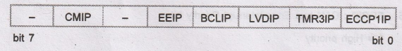
bit
7 Unimplemented : Read as '0'
bit
6 CMIP : Comparator Interrupt Priority bit
1
= High priority
0
= Low priority
bit
5 Unimplemented : Read as '0'
bit
4 EEIP : EEPROM Write Interrupt Priority bit
1
= High priority
0
= Low priority
bit
3 BCLIP : Bus Collision Interrupt Priority bit
1
= High priority
0
= Low priority
bit
2 LVDIP : Low-Voltage Detect
Interrupt Priority bit
1
= High priority
0
= Low priority
bit
1 TMR3IP : TMR3 Overflow Interrupt Priority bit
1
= High priority
0
= Low priority
bit
0 ECCP1IP : ECCP1 Interrupt Priority bit
1
= High priority
0
= Low priority
Fig.
18.16.13 Bit pattern for Peripheral Interrupt Priority Register 2
IPR3:
Peripheral Interrupt Priority Register 3
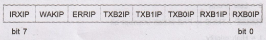
bit
7 IRXIP : Invalid Message Received Interrupt Priority bit
1
= High priority
0
= Low priority
bit
6 WAKIP : Bus Activity Wake-up Interrupt Priority bit
1
= High priority
0
= Low priority
bit
5 ERRIP : CAN bus Error Interrupt Priority bit
1
= High priority
0
= Low priority
bit 4 TXB2IP : Transmit Buffer 2 Interrupt
Priority bit
1
= High priority
0
= Low priority
bit
3 TXB1IP : Transmit Buffer 1 Interrupt Priority bit
1
= High priority
0
= Low priority
bit
2 TXBOIP : Transmit Buffer 0 Interrupt Priority bit
1
= High priority
0
= Low priority
bit
1 RXB1IP : Receive Buffer 1 Interrupt Priority bit
1
= High priority
0
= Low priority
bit
0 RXB0IP : Receive Buffer 0 Interrupt Priority bit
Introduction
to RISC Based Architecture
1
= High priority
0
= Low priority
Fig.
18.16.14 Bit pattern for Peripheral Interrupt Priority Register 3
e.
RCON Register
•
The Reset Control (RCON) register contains the IPEN bit which is used to enable
prioritized interrupts.

3. Priority of Interrupts
•
There are three Peripheral Interrupt Priority registers (IPR1, IPR2 and IPR3).
•
The Interrupt Priority (IPR) registers contain the individual priority bits for
the peripheral interrupts. They specify the priority of a particular request
either High or Low..
■
Priority Bit = 1 High Priority
■
Priority
Bit = 0 Low Priority
•
The high priority signals are located at program memory location 0008h and the
low priority signals at 0018h.
•
If the priority is disabled, by default, all the interrupts branch to 0008h
memory location.
•
Once the execution reaches the ISR, the interrupt is determined by polling the
interrupt flags and associated code sequence is executed. After execution of
code, the flag bit must be cleared in software to avoid recursion.
4. Programming of Timer using Interrupts
•
The timer interrupt is generated when the timer register overflows from FFh to
00h in 8-bit mode or FFFFh to 0000h in 16-bit mode. This overflow sets the
TMRXIF bit. The timer interrupt can be masked by clearing the TMRXIE bit.
•
The TMRXIF bit must be cleared in software by the Timer module Interrupt
Service Routine before re-enabling this interrupt.
•
Note: x may take value: 0, 1, 2, 3.
•
Table 18.16.1 shows the timers and their corresponding interrupt enable flag
bits and interrupt flag bits.

Steps
for Programming PIC18 Timer using Interrupt
1.
Enable GIE, PEIE, TMRXIE.
2.
Configure the TxCON register.
3.
Clear TMRXIF Timer interrupt flag.
4.
Load the count in Timer register TMRX
5.
Set TMRXON to start the Timer operation.
6.
When TMRXIF 1, code will jump to ISR to execute it, and after execution,
control returns to the main program.
Example
18.16.1 Write PIC18 Assembly program to transfer data
from Port B to Port C continuously and at the same time, generate a square wave
on pin PORTD.5
Solution
ORG
0000H
GOTO
MAIN ; Jump to new address to bypass interrupt vector
;
table
ORG
0008H ; Interrupt vector table
BTFSS
INTCON, TMROIF ; Check for Timer0 interrupt
RETFIE
; If not activated, return to main program
GOTO
TMR0_ISR ; If activated, execute Timer0 interrupt service
;
routine (ISR)
ORG
0100H ; Starting Main Program after interrupt vector table
;
space
MAIN
BCF TRISD, 5 ; Configure pin PD5 as an output
CLRF
TRISC ; Configure Port C as an output
SETF
TRISB ; Configure Port B as an input
MOVLW
08H ; Timer0, 16-bit, int clk, no prescalar
MOVWF
T0COM ; Load bit pattern in T0CON register
BACK MOVLW CFH ; W = CFH (Higher Byte)
MOVWF
TMR0H ; Load Higher byte in TMR0H
MOVLW
2CH ; W 2CH (Lower Byte)
MOVWF
TMR0L ; Load Lower byte in TMR0L
BCF
INTCON, TMR0IF ; Clear Timer interrupt flag bit
BSF
T0CON, TMR0ON ; Start Timer0
BSF
INTCON, TMR0IE ; Enable Timer0 interrupt
BSF
INTCON, GIE ; Enable interrupts globally
HERE MOVFF PORTB, PORTC ; Send data from Port B
to Port C continuously
BRA
HERE ;
TMR0_ISR
ORG
200H
MOVLW
CFH ; W = CFH (Higher Byte)
MOVWF
TMR0H ; Load Higher byte in TMR0H
MOVLW
2CH ; W = 2CH (Lower Byte)
MOVWF
TMR0L ; Load Lower byte in TMR0L
BTG
PORTD, 5 ; Toggle PD5
BCF
INTCON, TMR0IF ; Clear Timer0 interrupt flag bit
RETFIE
; Return from interrupt
END
Example
18.16.2 Write a C program for the PIC18 to generate a
square wave of 25 Hz frequency on RB4 using Timer0 ISR. Assume XTAL = 10 MHz.
Solution
:
Sol.
:
Given:
FOSC = 10 MHZ, No Prescaler
FTIMER
= FOSC / 4 = 10 / 4 = 2.5 MHZ
Period
= 1 / FTIMER = 1 / 2.5 MHz = 0.4 μs
T
= 1 / 25Hz = 0.04 s
TON
= TOFF = T / 2 = 0.02 s
Count
= Desired Delay Timer Priod = 0.02 s / 0.4 μs = 50000
The
value to be loaded in 16-bit Timer register is :
65536-Count
= 65536 - 50000 = 15536 = 3CB0H
#include
<P18F458.h>
void
Timer0_ISR(void);
void
CHK_ISR (void);
#define
PORTBit PORTBbits.RB4
#pragma
interrupt CHK_ISR
void
CHK ISR (void)
{
If
(INTCONbits.TMROIF 1) // If Timer0 caused interrupt execute Timer0_ISR
Timero_ISR();
}
#pragma
code HiPrio_Int = 0x08 // High priority interrupt
void
HiPrio_Int (void)
{
_asm
GOTO
CHK_ISR ; High priority interrupt land at address 0008H. To avoid using
;
limited memory space allocated to IVT and to have more space
;
for ISR we use GOTO instruction to CALL ISR written at
;
different place
_endasm
}
#pragma
code
void
main(void)
{
TRISBbits.TRISB4=0;
// configure pin 4 of Port B as output
INTCONbits.GIE
= 1; // Enable all interrupts globally
INTCONbits.PEIE
= 1; // Enable all peripheral interrupts
T0CON=0x08
// Timer0, 16 bit mode, no prescaler
INTCONbits.TMR0IF
= 0; // Clear Timer0 interrupt flag bit
TMR0H=0x3C;
// Load Higher byte in TMR0H
TMR0L=
0xB0; // Load Lower byte in TMR0L
INTCONbits.TMR0IE
= 1; // Enable Timer0 interrupt
T0CONbits.TMR0ON
= 1; // Start the Timer0
while(1);
// Wait for the interrupt
}
void
Timer0_ISR(void)
{
PORTBit
= ~PORTBit; // Toggle the bit RB4
TMR0H=0x3C;
// Load Higher byte in TMR0H
TMR0L=
0xB0; // Load Lower byte in TMR0L
INTCONbits.TMR0IF
= 0; // Clear Timer0 interrupt flag bit
}
Example
18.16.3 Write a C program for the PIC18 to generate a
square wave of 2 kHz frequency on RB4 using Timer0 ISR and a square wave of 5
kHz frequency on RB5 using Timer1 ISR. Assume XTAL = 10 MHz.
Solution:
Given: FOSC / 4 = 10 / 4 MHz, No Prescaler
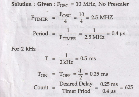
The
value to be loaded in 16-bit Timer0 register is :
65536
- Count = 65536 - 625 = 65911 = FD8FH
For
5 KHz
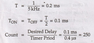
The
value to be loaded in 16-bit Timer1 register is:
65536-Count
= 65536 - 250 = 65286 = FF06H
#include
<P18F458.h>
void
Timer0_ISR(void);
void
CHK_ISR (void);
#define PORTBit1
PORTBbits.RB4
#define
PORTBit2 PORTBbits.RB5
#pragma
interrupt CHK_ISR
void
CHK ISR (void)
{
If
(INTCONbits.TMR0IF 1) // If Timer0 caused interrupt execute Timer0_ISR
Timer0_ISR();
If
(PIR1bits.TMR1IF = 1) // If Timer1 caused interrupt execute Timer1_ISR
Timer1_ISR();
}
#pragma
code HiPrio_Int = 0x08 // High priority interrupt
void
HiPrio_Int (void)
{
_asm
GOTO
CHK_ISR ; High priority interrupt land at address 0008H. To avoid using
;
limited memory space allocated to IVT and to have more space
;
for ISR we use GOTO instruction to CALL ISR written
;
at different place
_endasm
}
#pragma
code
void
main(void)
{
TRISBbits.
TRISB4=0; // configure pin 4 of Port B as output
TRISBbits.TRISB5=0;
//.configure pin 5 of Port B as output
INTCONbits.GIE
= 1; // Enable all interrupts globally
INTCONbits.PEIE
= 1; // Enable all peripheral interrupts
T0CON=0x08;
// Timer0, 16 bit mode, no prescaler
INTCONbits.
TMR0IF = 0; // Clear Timer0 interrupt flag bit
TMR0H=0xFD;
// Load Higher byte in TMR0H
TMR0L=
0x8F; // Load Lower byte in TMR0L
INTCONbits.TMR0IE
= 1 ; // Enable Timer0 interrupt
T1CON=0x88;
// Timer1, 16 bit mode, no prescaler
PIR1bits.TMR1IF
= 0; // Clear Timer1 interrupt flag bit
TMR1H=0xFF;
// Load Higher byte in TMR1H
TMR1L=
0x06; // Load Lower byte in TMR1L
PIE
1bits.TMR1IE = 1; // Enable Timer1 interrupt
TOCONbits.TMR0ON=1;
// Start the Timer0
T1CONbits.TMR1ON=1;
// Start the Timer1
while(1);
// Wait for the interrupts
}
void
Timer0_ISR(void)
{
PORTBit1=
~PORTBit1; // Toggle the bit RB4
TMR0H=0xFD;
// Load Higher byte in TMR0H
TMR0L=
0x8F; // Load Lower byte in TMR0L
INTCONbits.TMR0IF
= 0 ; // Clear Timer0 interrupt flag bit
}
void
Timer1_ISR(void)
{
PORTBit2
= ~PORTBit2; // Toggle the bit RB5
TMR1H=0xFF; // Load Higher byte in TMR1H
TMR1L=
0x06; // Load Lower byte in TMR1L
PIR1bits.TMROIF
= 0; // Clear Timer0 interrupt flag bit
}
5. Programming of External Hardware Interrupts
•
PIC18 microcontroller has three external hardware interrupts – INT0, INT1, and
INT2. They are on PORTB pins RB0, RB1, and RB2.
•
These interrupts are edge-triggered interrupts i.e. triggered by either a
rising edge or by a falling edge.
INTCON2:
Interrupt Control Register

INTEDG0
: External
Interrupt 0 Edge select bit
1
= Interrupt on Rising Edge
0=
Interrupt on Falling Edge
INTEDG1:
External
Interrupt 1 Edge select bit
1=
Interrupt on Rising Edge
0=
Interrupt on Falling Edge
INTEDG2:
External
Interrupt 2 Edge select bit
1=
Interrupt on Rising Edge
0=
Interrupt on Falling Edge
•
When a valid edge appears on the RBX/INTX pin, the corresponding flag bit
INTXIF is set. This interrupt can be disabled by clearing the corresponding
enable bit INTXIE. Flag bit INTXIF must be cleared in software in the Interrupt
Service Routine before re-enabling the interrupt.
•
Table 18.16.2 shows the external interrupts and their corresponding interrupt
enable flag bits and interrupt flag bits.

'steps
for Programming PIC18 External Interrupts
1.
Set PORTB External interrupt pin as an input.
2.
Also, make PORTB pins as digital input as it is multiplexed with ADC channels.
This is done by disabling the ADON bit in the ADCON1 register or by making the
PBADEN configuration a bit low.
3.
Configure INTCON2 register for edge trigger i.e. positive (rising) or negative
(falling) edge.
4.
Enable external interrupt (INTO, INT1, INT2) by setting a respective interrupt
to enable bit in the INTCON register.
5.
Enable Global Interrupt (GIE).
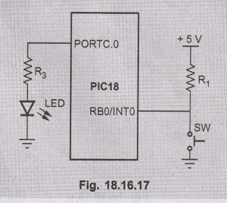
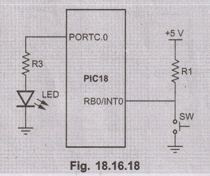
Example
18.16.4 Write PIC18 Assembly program to transfer data
from Port B to Port D continuously and at the same toggle the LED connected at
pin PORTC.0 upon activation of interrupt, INTO. The switch connected at pin
INTO (PORTB.0) generates an interrupt when pressed.
Solution
:
ORG
0000H
GOTO
MAIN Jump to new address to bypass interrupt vector
;
table
ORG
0008H ; Interrupt vector table
BTFSS
INTCON, INT0IF ; Check for INT0 interrupt
RETFIE
; If not activated, return to main program
GOTO
INT0_ISR ; If activated, execute INT0 interrupt service routine (ISR)
ORG
0100H ; Starting Main Program after interrupt vector table
;
space
MAIN BCF
TRISC, 0 ; Configure Pin PC0 as an output
CLRF
TRISD ; Configure Port D as an output
SETF
TRISB ; Configure Port B as an input
BSF
INTCON, INT0IE ; Enable INT0 interrupt
BSF
INTCON, GIE ; Enable interrupts globally
HERE MOVFF PORTB, PORTD ; Send data from Port B
to Port C continuously
BRA
HERE ;
INT0_ISR
ORG
200H
BTG
PORTC, 0 ; Toggle PC0
BCF
INTCON, INT0IF ; Clear INT0 interrupt flag bit
RETFIE
; Return from interrupt
END
Example
18.16.5 Write a C program for the PIC18 toggle the LED
connected to pin 0 of the PORT C every time INTO is activated by a switch
connected at INTO(RBO). Assume XTAL – 10 MHz.
Solution
:
#include
<P18F458.h>
void
INT0_ISR(void);
void
CHK_ISR (void);
#define
PORTBit PORTCbits.RC0
#pragma
interrupt CHK_ISR
void
CHK_ISR (void)
{
If
(INTCONbits.INT0IF = 1) // If INT 0
caused interrupt execute INT0_ISR
INT0_ISR();
}
#pragma
code HiPrio_Int = 0x08 // High priority
interrupt
void
HiPrio_Int (void)
{
_asm
GOTO
CHK_ISR ; High priority interrupt land at address 0008H. To avoid using
;
limited memory space allocated to IVT and to have more space
;
for ISR we use GOTO instruction to CALL ISR written at different place
_endasm
}
#pragma
code
void
main(void)
{
TRISBbits.TRISB0=1;
// configure pin 0 of Port B (INTO) as input
TRISBbits.TRISC0=0;
// configure pin 0 of Port C as output
INTCONbits.GIE
= 1; // Enable all interrupts globally
INTCONbits.INT0IF
: 0; // Clear INT0 interrupt flag bit
INTCONbits.INTOIE
= 1; // Enable INT0 interrupt
while(1);
// Wait for the interrupts
}
void
INT0_ISR(void)
{
PORTBit
= ~PORTBit; // Toggle the bit 0 of PORT C
INTCONbits.INTOIF
= 0; // Clear Timer0 interrupt flag bit
}
Review Questions
1. Draw and explain
the interrupt structure of PIC18?
2. Write a note on
enabling and disabling interrupts.
3. State the steps
to enable interrupts in PIC18.
4. Draw and explain
the bit pattern for INTCON register.
5. Draw and explain
the bit pattern for INTCON2 register.
6. Draw and explain
the bit pattern for INTCON3 register.
7. Draw and explain
the bit pattern for PIR1 register.
8. Draw and explain
the bit pattern for PIR2 register.
9. Draw and explain
the bit pattern for PIR3 register.
10. Draw and explain
the bit pattern for PIE1 register.
11. Draw and explain
the bit pattern for PIE2 register.
12. Draw and explain
the bit pattern for PIE3 register.
13. Draw and explain
the bit pattern for IPR1 register.
14. Draw and explain
the bit pattern for IPR2 register.
15. Draw and explain
the bit pattern for IPR3 register.
16. Write a short
note on interrupt priority in PIC18.
17. List the steps
for Programming PIC18 Timer using interrupt.
18. Explain the
programming of PIC18 Timer using interrupt with the help of an example.
19. List the steps
for Programming PIC18 external interrupts.
20. Explain the programming of PIC18 external Interrupts with the help of an example.
Microprocessors and Microcontrollers: Unit V: (b) Introduction to RISC Based Architecture : Tag: : - Interrupts and its Programming