Electron Devices and Circuits: Unit II: (b) Junction Field Effect Transistor (JEET)
JFET Amplifiers
• In the second chapter, we described the operation of JFET, and analysed and designed the d.c. response of circuits containing JFET. In this chapter we emphasize the use of FETs in linear amplifier applications.
JFET Amplifiers
AU
: May-03, 05, 09, 11, 14, Dec.-04, 05, 09
•
In the second chapter, we described the operation of JFET, and analysed and
designed the d.c. response of circuits containing JFET. In this chapter we
emphasize the use of FETs in linear amplifier applications.
•
JFET amplifiers provide an excellent voltage gain with the added advantages of
a high input impedance. Because of their high input impedance and other
characteristics JFETs are often preferred over BJTs for certain types of
applications.
•
Many of the concepts that relate to amplifiers using BJTs apply equally to FET
amplifiers. There are three basic FET circuit configurations :
•
Common source • Common drain and • Common gate
•
These are similar to the bipolar transistor common emitter, common collector
and common base circuits, respectively. The only difference is that BJT
controls a large output (collector) current by means of a relative small input
(base current), whereas, FET controls an output (drain) current by means of
small input (gate) voltage. It is important to note that in both the cases the
output current is the controlled variable.
1. JFET as an Amplifier
•
Field-effect transistor amplifier circuits use the voltage-controlled nature of
the JFET. In the pin ch-off region, ID depends (approximately) only on VGS
•
Let us discuss the use of the JFET as an amplifier by considering the
common-source circuit, shown in the Fig. 3.9.1.

•
The voltage VGG provides the necessary reverse-bias between gate and
source of the JFET. The signal to be amplified is Vs. The V-I characteristics
of the JFET is as shown in Fig. 3.9.2.

•
On the output characteristics, a load line corresponding to VDD = 40 V and RD =
8 kQ is constructed. The transistor is biased at point Q and results in VDSQ =
20 V and IDQ = 2.70 mA.
•
Assuming that the signal voltage Vs is a sinusoid of peak voltage Vm = 0.5 V,
this signal is superimposed on the quiescent level. The instantaneous gate-to
source voltage is
Vgs
= Vs - VGG
•
The resulting waveforms for ID and VDS are as shown in Fig. 3.8.2.
•
Both quantities, ID and VDS, can be considered as sinusoids superimposed on the
d.c. values.
Then VGS = - V GG + Vgs =
-1.5 + 0.5 sin ωt
ID
= IDQ + id = 2.70 + 0.5 sin ωt
mA
Vout
= VDS = VDSQ + VdS = 20 + 4 sin ωt
•
We observe that the output signal is greater than the input signal, thus
indicating amplification.
•
The magnitude of the voltage gain |Av | is the ratio of the output a.c. signal
amplitude [4.0 V] to the input a.c. signal amplitude [0.5 V]. Then, in this
example,
|AV|
= 4.0 / 0.5 = 8
•
Note that the quiescent operating point Q is selected approximately at the
midpoint of the load line. This gives undistorted output, i.e. output waveform
is sinusoidal when the input signal is sinusoidal. If the operating point is
selected either close to the ohmic region or near the pinch-off voltage, i.e.
at the one of the ends of the load line, the output sinusoid would be clipped
during either the positive or negative half-cycles of the input signal. In case
of common-source circuit of JFET, there is a phase shift of 180° between the
input and output sinusoidal voltages.
2. Small Signal A.C. Equivalent Circuit for JFET
•
The JFET parameters are the major components of low frequency small signal
model for JFET. We know that, drain to source current of JFET is controlled by
gate to source voltage. The change in the drain current due to change in gate
to source voltage can be determined
using the transconductance factor gm. It is given as
Δ
Id = gm Δ VGS ...(3.9.1)
•
We know that, in BJT the relation between an output and input quantity is given
by amplification factor P, whereas in JFET this relation is given by
transconductance factor g m.
•
The another important parameter of JFET is drain resistance rd . It is given by

•
It determines the output impedance Zo of the JFET amplifier.
•
The amplification factor u of an FET is defined as

•
The parameters gm, rd and u are related by,
µ
= rd gm
JFET
Low Frequency a.c. Equivalent Circuit
•
Fig. 3.9.3 shows the small signal low frequency a.c. equivalent circuit for
n-channel JFET. The relation of Id by Vgs is included as a current source gmVgs
connected from drain to source. The input impedance is represented by the open
circuit at its input terminals, since gate current IG is zero. The output
impedance is represented by rd from drain to source.

Key
Point : The lower case subscripts represent a.c. levels.
Approximate
a.c Equivalent Circuit
•
When the value of external drain resistance RD is very small as compared to the
value of output impedance represented by rd, it is possible to replace rd by
open circuit. This gives us approximate ac equivalent circuit of JFET
amplifier, as shown in Fig. 3.9.4.

3. Common Source Amplifier with Fixed Bias
•
Fig. 3.9.5 shows common source amplifier with fixed bias. The coupling
capacitor Cx and C2 which are used to isolate the d.c. biasing from the applied
ac signal act as short circuits for the ac analysis.
•
Fig. 3.9.5 shows the low frequency equivalent model for the common source
amplifier circuit with fixed bias. It is drawn by replacing :
•
All capacitors and d.c. supply voltages with short circuits and
•
JFET with its low frequency equivalent circuit.
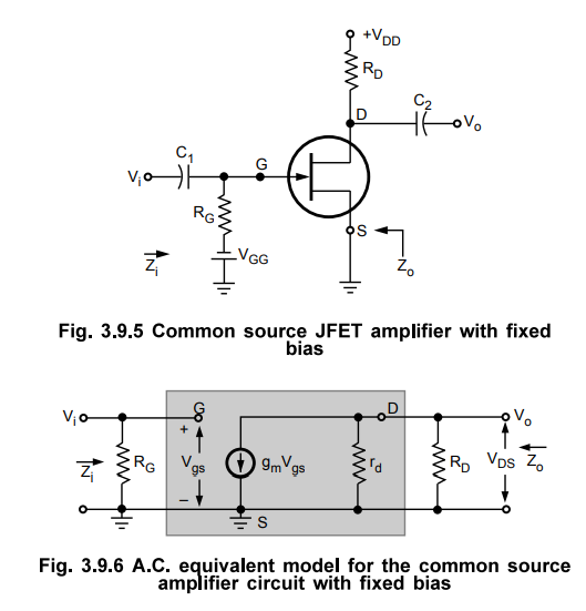
•
Now, we see the input impedance output impedance and voltage gain of the above
model.
Input
Impedance Zi:
Looking
into Fig. 3.9.5 we can say that,
Zi
= RG ... (3.9.4)
Output
Impedance Zo:
•
The output impedance Zo is the impedance measured looking
from the output side with input voltage (Vi) equal to 0. As Vi
= 0,
Vgs
= 0 and hence gm Vgs = 0
•
The gm Vgs = 0 allows current source to be replaced by an open circuit, as
shown in the Fig. 3.9.7.

Therefore
the output impedance is,
Zo
= RD ||rd … (3.9.5)
•
If the resistance r is sufficiently large compared to RD, then we
say that the output impedance is approximately equal to RD.
Zo
≈ RD rd >> RD … (3.9.6)
Voltage
Gain Av :

Key
Point : The negative sign in the equation for Av clearly
indicates there is a phase shift of 180° between input and output voltages.
•
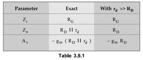
Table 3.8.1 summarizes performance of common source amplifier with fixed bias.
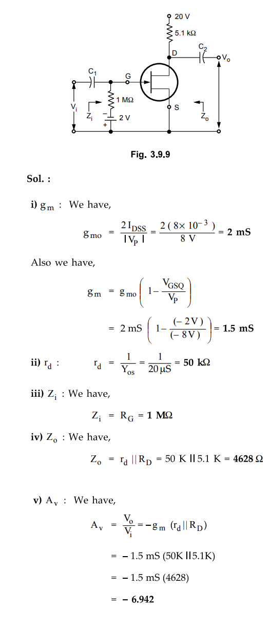
Ex.
3.9.1 For the circuit shown in Fig. 3.9.8. Determine i) Input impedance ii) Output impedance and iii) Voltage gain.

Sol.
: i) We have,
Zi
= RG = 1 MΩ
ii)
We have, Zo = rd ||RD = 50 K 115.1 K = 4628 Ω
iii)
Voltage Gain Av : We have,
Av
= -gm (rd ||RD )
=
-2 mS (50 K 115.1 K)
=
- 2 mS (4628) = - 9.256
Ex.
3.9.2 For the circuit shown in the Fig. 3.9.9 VGSQ = -2 V with IDSS = 8 mA and
VP=-8V. Calculate gm, rd, Zir Zo and Ay. The value of Yos is given as 20 µS.
4. Common Source Amplifier with Self Bias (Bypassed Rs)
•
Fig. 3.9.10 shows common source amplifier with self bias.
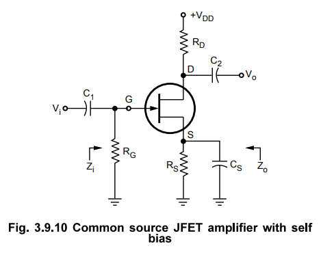
•
The coupling capacitor C1 and C2 which are used to
isolate the d.c. biasing from the applied a.c. signal act as short circuits for
the low frequency analysis. Bypass capacitor Cs also acts as a short circuit
for the low frequency analysis.
•
Fig. 3.9.11 shows the low frequency equivalent model for the common source
amplifier circuit with self bias. It is drawn by replacing
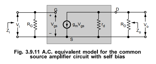
•
All capacitors and d.c. supply VDD with short circuits and,
•
JFET with its low frequency equivalent circuit.
•
Since the resulting low frequency equivalent circuit is same as a.c. equivalent
circuit in Fig. 3.9.6, the equation for Z;, Zo and Av will also be same.
i)
Input impedance Zi :
Zi
= RG ... (3.9.11)
ii)
Output impedance Zo :
Zo
= rd||RD ...(3.9.12)
if
rd >> RD
Zo
≈ RD ... (3.9.13)
iii)
Voltage gain Av :
Av
= -gm (rd ||RD ) ... (3.9.14)
If
rd >> R D
Av
= “gm RD ... (3.9.15)
• The negative sign in the equation (3.9.11) and (3.9.12) again indicates there is a phase shift of 180° between input and output voltages.
Electron Devices and Circuits: Unit II: (b) Junction Field Effect Transistor (JEET) : Tag: : - JFET Amplifiers
Related Topics
Related Subjects

Electron Devices and Circuits
EC3301 3rd Semester EEE Dept | 2021 Regulation | 3rd Semester EEE Dept 2021 Regulation