Electron Devices and Circuits: Unit II: (b) Junction Field Effect Transistor (JEET)
Junction Field Effect Transistor (JFET)
Structure of Channel
• Heavily doped electrodes of p type material form p-n junctions on each side of the bar. The thin region between the two p gates is called the channel. Since this channel is in the n type bar, the FET is known as n-channel JFET.
Junction Field Effect Transistor
1. Structure of n-Channel JFET
•
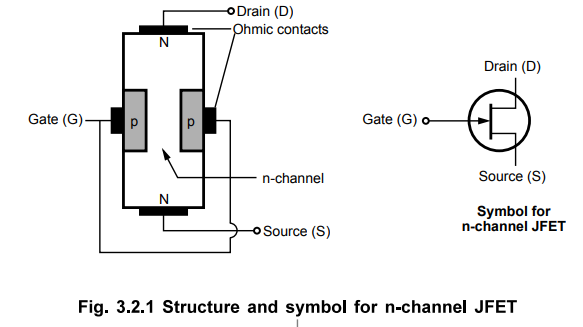
The Fig. 3.2.1 shows structure and symbol of n-channel JFET. A small bar of
extrinsic semiconductor material, n type is taken and at its two ends, two
ohmic contacts are made which are the drain and source terminals of FET.
•
Heavily doped electrodes of p type material form p-n junctions on each side of
the bar. The thin region between the two p gates is called the channel. Since
this channel is in the n type bar, the FET is known as n-channel JFET.
•
The electrons enter the channel through the terminal called source and leave
through the terminal called drain. The terminals taken out from heavily doped
electrodes of p type material are called gates. Usually, these electrodes are
connected together and only one terminal is taken out, which is called gate, as
shown in the Fig. 3.2.1.
2. Structure of p-Channel JFET
•
The device could be made of p type bar with two n type gates as shown in the
Fig. 3.2.2. Then this will be p-channel JFET.
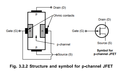
• The principle of working of n-channel JFET
and p-channel JFET is similar; the only difference being that in n-channel JFET
the current is carried by electrons while in p-channel JFET, it is carried by
holes.
Electron Devices and Circuits: Unit II: (b) Junction Field Effect Transistor (JEET) : Tag: : Structure of Channel - Junction Field Effect Transistor (JFET)
Related Topics
Related Subjects

Electron Devices and Circuits
EC3301 3rd Semester EEE Dept | 2021 Regulation | 3rd Semester EEE Dept 2021 Regulation