Electron Devices and Circuits: Unit IV: Multistage and Differential Amplifiers
Methods of improving CMRR
Differential Amplifiers
• Higher the value of CMRR, better is the performance of differential amplifier. Hence in practice the efforts are always to improve the CMRR of the differential amplifier.
Methods of Improving CMRR
AU
: Dec.-15, May-17
•
Higher the value of CMRR, better is the performance of differential amplifier.
Hence in practice the efforts are always to improve the CMRR of the
differential amplifier.
1. Effect of RE
•
To improve the CMRR, the common mode gain A must be reduced. 8.9.1
•
The common mode gain Ac approaches zero as RE tends to infinity. This is
because RE introduces a negative feedback in the common mode operation which
reduces the common mode gain Ac.
•
Thus higher the value of RE, lesser is the value of A c and higher is the value
of CMRR.
•
The differential gain Ad is not dependent on RE
•
But practically RE cannot be selected very high due to certain limitations such
as,
1.
Large RE needs higher biasing voltage to set the operating Q point
of the transistors.
2.
This increases the overall chip area.
•
Hence practically instead of increasing RE various other methods are used which
provide effect of increased RE without any limitations. Such two
methods are –
1.
Constant current bias method, and
2.
Use of current mirror circuit.
•
The other method used to increase Ad to improve CMRR is called use
of an active load.
2. Differential Amplifier with Constant Current Source
AU
: May-09, 10, 11, 12, 13, Dec.-07, 11
•
Without physically increasing the value of RE, the RE is replaced by a
transistor operated at a constant current.
•
Such a constant currrent source circuit gives the effect of a very high
resistance without affecting the Q point values of the differential amplifier.
•
The differential amplifier using constant current bias circuit instead of RE is
shown in the Fig. 8.9.1.
•
The transistor used is Q 3 and the values of Rx, R2 and R3 are selected so as
to give the same operating point values for the two transistors Q1 and Q2.
a.
Circuit Analysis
•
Let current through R3 be IE3 while current through R3 is
I.
•
Neglecting the base current of Q3 which is very small due to large
Pac, we can assume that current through R2 is also I.
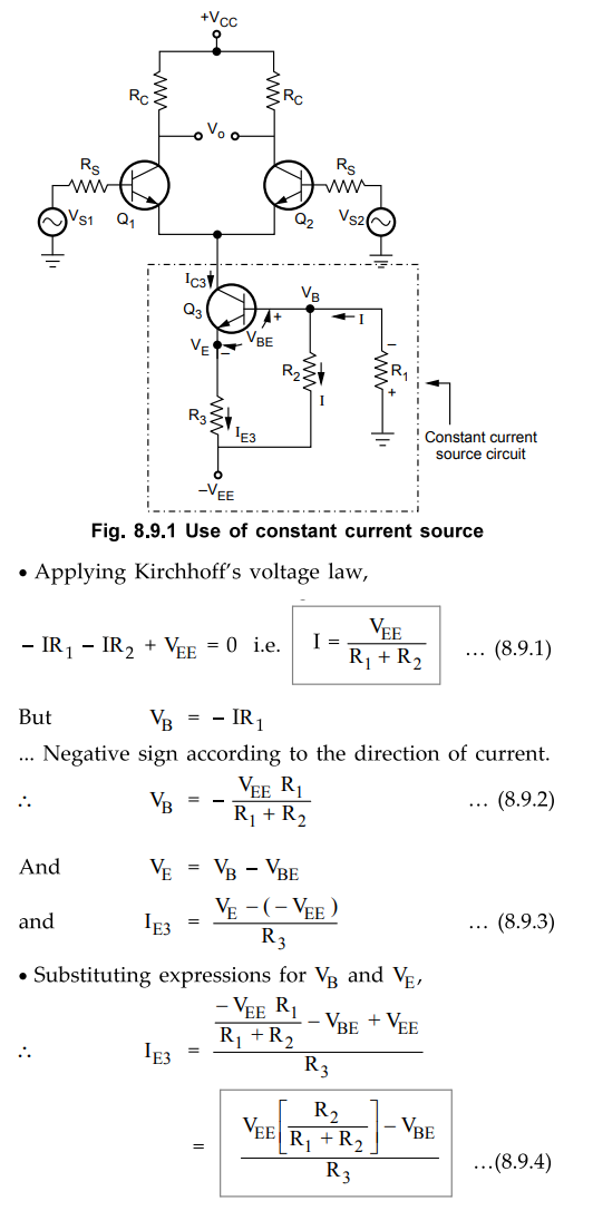
•
Neglecting IB3 we can write , IC3 = IE3
•
Thus as VEE, R1 , R2 , R3 and VBE
are constants, current IC3 is almost equal to IE3 and
also constant. Thus circuit with transistor Q3, acts as a constant
current source.
Key
Point : The internal resistance of a constant current
source is very high, ideally infinite. Hence this circuit makes the value of
emitter resistance ideally infinite which reduces the common mode gain Ac
ideally to zero.
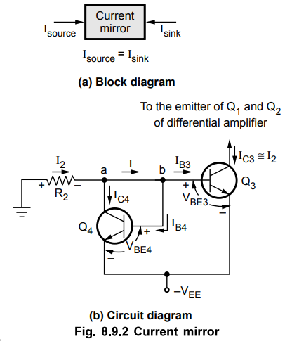
3. Current Mirror Circuit
•
The circuit in which the output current is forced to equal the input current is
called current mirror circuit.
•
In a current mirror circuit, the output current is the mirror image of input
current.
•
The basic block diagram is shown in Fig. 8.9.2 (a) while the Fig. 8.9.2 (b)
shows the circuit diagram.
 a.
Circuit Analysis
a.
Circuit Analysis
•
The circuit consists of two matched transistors Q 3 and Q4. Their base-emitter
voltage and base currents are same.
VBE3
= VBE4 and IB3 = IB4
Similarly
their collector currents are also same.
i.e.
Ic3 = Ic4
Applying
KCL at node a,
I2
= Ic4 + I … (8.9.5)
Applying
KCL at node b,
I
= IB3 + IB4 = 2IB4 = 2IB3 … (8.9.6)
Generally
β is very large and hence (2/ β) is negligibly small.
I2
≅ IC3 … (8.9.9)
•
Thus the collector current of Q 3 is nearly equal to the current I2.
•
Hence once current mirror circuit is set for current I2, it provides constant
current bias to the differential amplifier.
•
Thus I2 can be obtained by writing KVL for the base-emitter loop of
transistor Q 3.
•
Selecting R2, the appropriate I2 can be set for the
current mirror circuit.
b.
Advantages
•
The various advantages of current mirror circuit are,
1.
Provides very high emitter resistance RE-
2.
Requires less components that constant current bias.
3.
Simple to design.
4.
Easy to fabricate.
5.
With properly matched transistors, collector current thermal stability is
achieved.
•
Thus constant current bias can be easily replaced by current mirror circuit to
improve CMRR.
•
Due to its advantages, current mirror circuit is most commonly used in the
integrated circuit op-amps.
4. Use of an Active Load to Improve CMRR
•
To imporove CMRR, it is necessary to increase Ad
•
To increase Ad, RC must be high as possible as
Ad
= RC/re
•
But there are limitations to select maximum value of RC such as :
i)
For large RC the quiescent drop is more hence higher biasing voltage
is necessary to maintain the quiescent collector current.
ii)
Higher value of RC requires a large chip area. Hence it is not possible
to increase the value of RC beyond a particular limit.
•
The current mirror circuit has very low d.c. resistance (dV/dI) and higher a.c.
resistance (dv/di)
•
The requirement to increase the gain is same that the collector resistance
should not disturb d.c. conditions while it must provide large resistance for
a.c. purposes.
•
Hence the current mirror circuit can be used as a collector load instead of RC.
Such a load is called an active load.
•
The quiescent voltage across the current mirror is the fraction of the supply
voltage. This eliminates the need of high biasing supply voltage.
•
The differential amplifier using a current mirror as an active load is shown in
the Fig. 8.9.3.
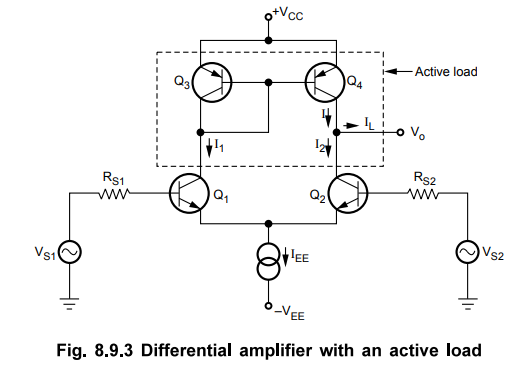
•
Under the d.c. conditions, VS1 = VS2 = 0. As Q1
and Q2 are matched transistors hence I1 =I2 =
IEE /2, where base currents of Q1 and Q2 are
neglected.
•
The transistors Q3 and Q4 form a current repeater hence I = I1 = I2.
•
The load current IL entering the next stage is,
IL
= I – I2 = 0 ... (8.9.11)
•
But when VS1 increases over VS2' the current Ix increases
whereas I2 decreases as I1 + I2 = IEE
constant.
•
Also the current I always remains equal to I1 due to the current
mirror action.
Key
Point : Thus the active load provides very high
a.c. resistance and hence high differential mode voltage gain. Thus as Ad
becomes high, CMRR gets improved.
5. JFET Differential Amplifier
•
Fig. 8.9.4 shows a basic JFET differential pair biased with a constant-current
source.
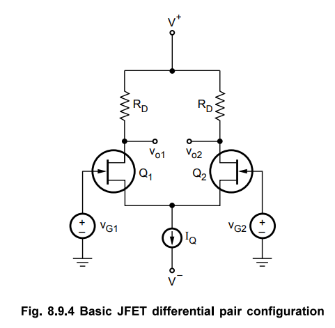
•
If a pure differential-mode input signal is applied such that vG1 = + vd/2 and
vG2 = -vd/2, then drain currents IDI and ID2 increases and decreases,
respectively, in exactly the same way as in the MOSFET differential amplifier.
•
Fig. 8.9.5 shows the equivalent circuit, with the output resistance of the
constant-current source and the small-signal resistances of Qi and Q2 assumed
to be infinite.
•
The small-signal equivalent circuit of the JFET differential amplifier is
identical to that of the MOSFET differential amplifier for the case when the
current-source output resistance is infinite. Applying KCL of common source
node we have
gm
Vgs1 + gm Vgs2 =0 ...(8.9.12)
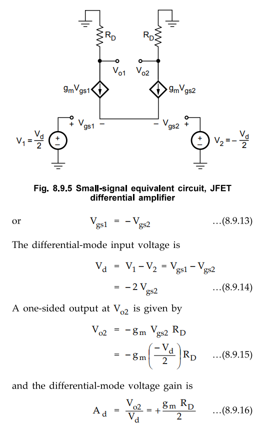
•
The expression for the differential-mode voltage gain for the JFET differential
amplifier is exactly the same as that of the MOSFET differential amplifier. If
the constant-current source output resistance is finite, then the JFET
differential amplifier will also have a nonzero common-mode voltage gain.
Review Questions
1. State the methods of improving CMRR of a differential
amplifier.
2. Justify how a constant current source is used in place of RE
to improve the CMRR for a differential amplifier.
3. Explain the working of current mirror circuit with necessary
derivations.
4. With the help of neat circuit diagram explain the working of active load for differential amplifier.
AU : Dec.-15, Marks 8
5. Draw the JFET differential amplifier and derive the
expressions for Ad.
6. Draw the circuit diagram and explain the working of a
differential amplifier using FET. Derive the expression for differential mode
gain and common mode gain.
AU : May-17, Marks 13
Electron Devices and Circuits: Unit IV: Multistage and Differential Amplifiers : Tag: : Differential Amplifiers - Methods of improving CMRR
Related Topics
Related Subjects

Electron Devices and Circuits
EC3301 3rd Semester EEE Dept | 2021 Regulation | 3rd Semester EEE Dept 2021 Regulation