Linear Integrated Circuits: Unit IV: Special ICs
Monolithic Phase Locked Loop IC 565
Operating working principle, Block Diagram, Pin Diagram, Functions of Pins, Working functions, Solved Example Problems
These ICs are differ mainly in operating frequency range, power supply requirements, and frequency and bandwidth adjustment ranges. IC 565 PLL is most commonly used and hence discussed in this section.
Monolithic Phase Locked Loop IC 565
Monolithic
PLLs are introduced by signetics as SE/NE 560 series and by National
semiconductor as LM 560 series. The SE/NE 560 series includes SE/NE 560, 561,
562, 564, 565 and 567. These ICs are differ mainly in operating frequency
range, power supply requirements, and frequency and bandwidth adjustment
ranges. IC 565 PLL is most commonly used and hence discussed in this section.
1. IC 565
IC
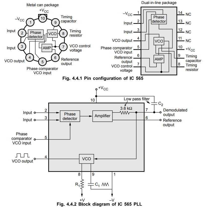
565 is available in a 14 pin DIP package and 10 pin metal can package. Fig.
4.4.1 shows 14-pin package configuration for IC 565 and Fig. 4.4.2 shows the
block diagram for IC 565.
The
block diagram of IC 565 PLL consists of phase detector, amplifier, low pass
filter and VCO. As shown in the block diagram the phase locked feedback loop is
not internally connected. Therefore, it is necessary to connect output of VCO
(pin 4) to the phase comparator input (pin 5), externally. In frequency
multiplication applications a digital frequency divider is inserted into the
loop i.e. between pin 4 and pin 5.
The
centre frequency of the PLL is determined by the free-running frequency of the
VCO and it is given as
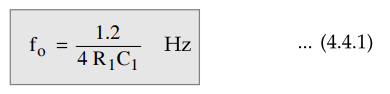
where
R1 and C1 are an external resistor and a capacitor
connected to pins 8 and 9, respectively. The values of R1 and C1
are adjusted such that the free running frequency will be at the centre of the
input frequency range. The value of R1 is restricted from 2 kΩ to 20
kΩ, but a capacitor can have any value. A capacitor C2 connected
between pin 7 and the positive supply (pin 10) forms a first order low pass
filter with an internal resistance of 3.6 kΩ. The value of filter capacitor C2
should be large enough to eliminate possible oscillations in the VCO voltage.
The
lock range and capture range for IC 565 PLL are given by the following
equations:
where
C2 is in farads
From
equation 4.4.2 we can notice that lock range increases with an increase in
input voltage but decreases with increase in supply voltage. The two inputs
(pin 2 and pin 3) to the phase detector allows direct coupling of an input
signal, provided that there is no dc voltage difference between the pins and the
dc resistances seen from pins 2 and 3 are equal. A reference voltage at pin 6
is approximately equal to the dc voltage of the demodulated output at pin 7.
This reference voltage may be used as comparator input in applications like
frequency shift keying will be discussed in section 4.5.
Example
4.4.1 For the circuit shown in the Fig. 4.4.3, calculate
free running frequency, lock range and capture range.
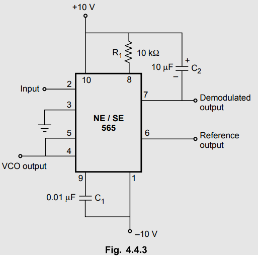
Solution
:
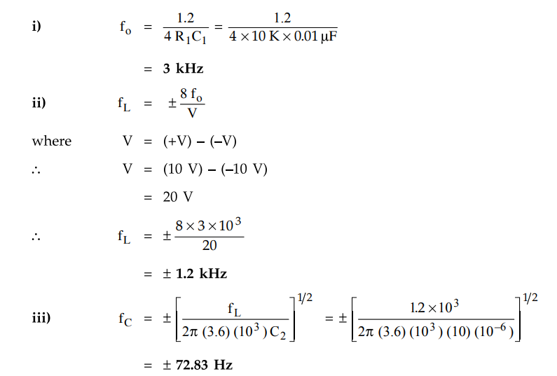
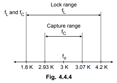
Fig.
4.4.4 shows the relationship between fo, fL and fC.
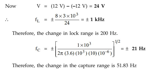
Example
4.4.2 For circuit shown in Fig. 4.4.3,
calculate the change in lock and capture range
if
supply voltages are changed as follows :
V=
12 V and -V = -12 V
Solution
:
We know that, fo = 3 kHz (calculated in the previous problem)
2. Derivation of LOCK Range
The
Fig. 4.4.5 shows the block diagram to determine lock-range.
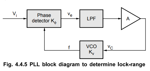
Looking
at Fig. 4.4.5, let us assume that the output voltage of the phase detector is
Ve
= K ϕ
(θe - π / 2) where θe
= Phase error ... (4.4.4)
The
output voltage of the phase detector is filtered by the low-pass filter to
remove the high frequency components. The output of the filter is amplified by
a gain A and then applied as the control voltage VC to the VCO as
given by,
vC
= Ave = Kϕ A(θe - π
/2) ...(4.4.5)
This
control voltage vC will result in a shift in the VCO frequency from
its center frequency f0 to a frequency f, given by
f
= fo + Kv vC
When
the PLL is locked into the input signal frequency fi? we have
f
= fi = fo + Kv vC ...(4.4.6)
Substituting
value v c from equation (4.4.5) we have,
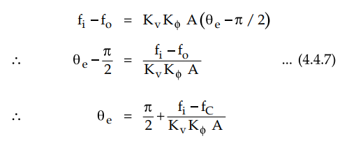
The
maximum output voltage magnitude available from the phase detector occurs for ϕ
= π and 0 radian and is
ve(max)
= ± Kϕ (π /2)
The
corresponding value of the maximum control voltage available to drive the VCO
will be
vC(max)
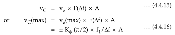
= ± Kϕ (π /2) A ...(4.4.8)
Substituting
the maximum value of v C from equation (4.4.8) in equation (4.4.6) we have,
f
= fi = fo ± KvKϕ (π /2)A
fo
± ΔfL
where
2 ΔfL will be lock-in frequency range given by,
Lock
range = 2 ΔfL = KvKϕ A π ΔfL = KvKϕ A
π/2
The
lock-in range is symmetrically located with respect to VCO free running
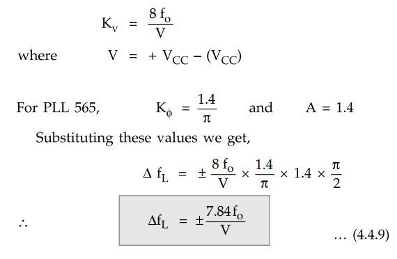
frequency fo. For PLL 565,
we
have
3. Derivation of Capture Range
The
capture range is the range of input frequencies for which the initially
unlocked loop will lock on an input signal. Thus is always less than the lock
range. Since capture range, Δ ωcap denotes a transient
condition, it is not as readily derived as a lock-in range. However, an
approximate parametric expression for the capture range will be initially
derived to give an estimate of the capture range. It can be derived by
employing simple lag filter. When PLL is not locked the phase angle difference
between the signal and the VCO output voltage is given by

The
phase angle difference thus not be constant, but will change with time at a
rate given by
dθe
/ dt = ωs - ωo (4.4.11)
The
phase detector output voltage will therefore not have a dc component, but
rather will have an ac voltage with a triangular waveform of peak amplitude K
(л/2) and the fundamental frequency of ωs - ωo i.e. fs
- fo = Δf.
Let
us derive an approximate expression for capture range for PLL employing a
simple lag filter. The transfer function for a simple lag filter is given by,
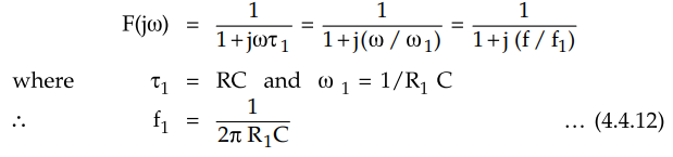
For
the condition that (f/f1)2 >> 1, the transfer
function can be expressed approximately as
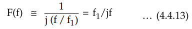
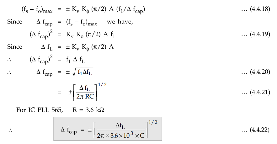
The fundamental input frequency term supplied to the low pass filter by the phase detector will be at the difference frequency Δf = fs - fo. If Δf > 3f1 the transfer function of LPF will be approximately given by,
F(Δf)
= f1 / Δf = f1 /( fs - fo) ...(4.4.14)
The
voltage available to drive the VCO is given by,
The
corresponding value of the maximum frequency shift will be given by,

For
the acquisition of the signal frequency fs, we must have that f = fs so that
the maximum signal frequency range can be required by the PLL will be,
The
total capture range is 2 A fcap.
Review Questions
1. Show that the
lock-in range of a PLL is given by AfL = ~ V ° w^iere symbols used have the
usual meaning.
Dec.-03, 11, Marks 8
2. Derive the
expression for capture range for PLL where a simple RC network is used as a low
pass filter.
Dec.-l0, Marks 8
3. Briefly explain the
functional block diagram of PLL IC 565.
Dec.-08,09, May-17,
Marks 16
Linear Integrated Circuits: Unit IV: Special ICs : Tag: 3. Derivation of Capture Range : Operating working principle, Block Diagram, Pin Diagram, Functions of Pins, Working functions, Solved Example Problems - Monolithic Phase Locked Loop IC 565
Related Topics
Related Subjects

Linear Integrated Circuits
EE3402 Lic Operational Amplifiers 4th Semester EEE Dept | 2021 Regulation | 4th Semester EEE Dept 2021 Regulation