Electron Devices and Circuits: Unit III: (b) MOSFET Amplifier
MOSFET Small Signal Model
Equivalent circuit, Solved Example Problems
• The output voltage is also a combination of d.c. and a.c. values. The time-varying output signal is the time-varying drain-to-source voltage, or Vo = Vds = - idRD
MOSFET Small Signal Model
•
From Fig. 7.1.1, we see that the output voltage is
VDS
= Vo = VDD - iD RD
•
Using equation (7.2.6) of section 7.2 , we obtain
Vo
= VDD - (IDQ + id)RD
=
(VDD - IDQ RD) - id RD
•
The output voltage is also a combination of d.c. and a.c. values. The
time-varying output signal is the time-varying drain-to-source voltage, or
Vo
= Vds = - idRD ...(7.3.3)
•
Also, from equations (7.2.6) and (7.2.7) of section 7.2, we have
id
= gm Vgs
•
In summary, the following relationships exist between the time-varying signals
for the circuit in Fig. 7.1.1 (a). The equations are given in terms of the
instantaneous a.c. values, as well as the phasors. We have,

•
The Fig. 7.3.1 shows the a.c. equivalent circuit. Here, the d.c. sources in
Fig. 7.1.1 are made zero.

•
From the equivalent circuit for the NMOS amplifier circuit, we can draw a small
signal equivalent circuit for the MOSFET.
•
The Fig. 7.3.2 (b) shows the small signal low frequency a.c. equivalent circuit
for n-channel MOSFET.
•
The relation of Id by Vgs is included as a current source gmv gs connected from
drain to source.

•
The input impedance is represented by the open circuit at its input terminals,
since gate current IG is zero.
•
We know that the circuit has the finite output resistance of a MOSFET biased in
the saturation region because of the nonzero slope in the ip versus VDS curve.
We also know that,
iD
= K[(vGS-VT)2(1+ λvDS)] ... (7.3.8)
where
λ is the channel-length modulation
parameter and is a positive quantity. The small signal output resistance, is
defined as,

•
This small signal output resistance is also a function of the Q-point
parameters. The Fig. 7.3.3 shows the small signal equivalent circuit of
common-source circuit shown in Fig. 7.1.1.

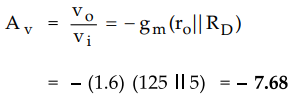
Ex.
7.3.1 For the circuit shown in Fig. 7.3.4. MOSFET parameters are: VT
= 1 V, K = 0.80 mA/V2, and λ = 0.01 VT -1. Determine the
small signal voltage gain of a MOSFET circuit. Assume the transistor is biased
in the saturation region.
Sol.
:
Step
1:
Calculate IDQ gm and ro
The quiescent values are,

Step
2:
Draw the small signal ac equivalent circuit.

Step
3:
Calculate voltage gain
Look
at Fig. 7.3.5, we have
Vo
= -gm Vgs (ro
||RD)
Since
vgs = Vi,
The
small signal voltage gain is,
Ex.
7.3.2 For the circuit shown in Fig. 7.3.6, if VTN = 1 V, Kn
= 0.8mA/V2, λ = 0.01 V-1, determine small signal voltage
gain. Assume that EMOSFET is biased in saturation and VGSQ = 3V

Sol.
:
Step
1 :
Calculate IDQ , gm and Io

Ex.
7.3.3 Determine the small signal voltage gain of a MOSFET circuit shown in Fig.
7.3.7. Assume VGSQ = 2.12 V, VDD = 5 V, RD = 2.5 kQ. Assume transistor parameters
are VT = 1 V, K = 0.80 mA/V7 and λ = 0.02/V. Assume the transistor biased in
the saturation region.
 Sol
.:
Sol
.:
The
quiescent Values are,

Important Concept
•
Because of the relatively low value of transconductance, MOSFET circuits tend
to have a lower small signal voltage gain than comparable bipolar circuits.
•
The negative sign in the gain indicates that the sinusoidal output voltage is
180 degrees out of phase with respect to the input sinusoidal signal.
1. Steps in the A.C. Analysis of MOSFET Amplifier
•
The steps to be performed in the analysis of the MOSFET amplifier are as
follows:
1.
Perform the d.c. analysis of the circuit and check whether the MOSFET is biased
in the saturation region in order to produce a linear amplifier.
2.
Replace the MOSFET by its small signal equivalent circuit.
3.
Analyze the small signal equivalent circuit, making the d.c. source components
equal to zero.
2. CS MOSFET Amplifier with p-channel MOSFET
•
The Fig. 7.3.8 shows the common source circuit with p-channel MOSFET and its
a.c. equivalent circuit.
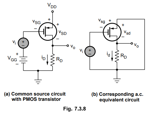
•
The a.c. equivalent circuit seen for n-channel MOSFET also applies to the
p-channel MOSFET; however, there is a change in current directions and voltage
polarities compared to the circuit containing the n-channel MOSFET.
•
The Fig. 7.3.9 shows the small signal equivalent circuit of the p-channel
MOSFET amplifier.

Important
Concept
•
It is important to note that the expression for the small signal voltage gain
of the p-channel MOSFET amplifier is exactly the same as that for the n-channel
MOSFET amplifier.
•
The negative sign indicates that a 180- phase reversal exists between the
output and input signals, for both the PMOS and the NMOS circuits.
Review Questions
1. Draw and explain the small signal equivalent circuit of
MOSFET.
2. Describe about small signal MOSFET amplifiers (NMOS) and
obtain the expression for it's transconductance.
Electron Devices and Circuits: Unit III: (b) MOSFET Amplifier : Tag: : Equivalent circuit, Solved Example Problems - MOSFET Small Signal Model
Related Topics
Related Subjects

Electron Devices and Circuits
EC3301 3rd Semester EEE Dept | 2021 Regulation | 3rd Semester EEE Dept 2021 Regulation