Electron Devices and Circuits: Unit IV: Multistage and Differential Amplifiers
Multistage Amplifiers
Equivalent circuit, Solved Example Problems
• In practice, we need amplifier which can amplify a signal from a very weak source such as a microphone, to a level which is suitable for the operation of another transducer such as loudspeaker. This is achieved by cascading number of amplifier stages, known as multistage amplifier or Casceded amplifier.
Multistage Amplifiers
AU
: Dec.-02,03,09,10,12,14, May-03,05,09,10,11, Marks 16, May-15, Marks 2
•
In practice, we need amplifier which can amplify a signal from a very weak
source such as a microphone, to a level which is suitable for the operation of
another transducer such as loudspeaker. This is achieved by cascading number of
amplifier stages, known as multistage amplifier or Casceded amplifier.
1. Need for Caacading
•
For faithful amplification amplifier should have desired voltage gain, current
gain and it should match its input impedance with the source and output
impedance with the load. Many times these primary requirements of the amplifier
cannot be achieved with single stage amplifier, because of the limitation of
the transistor/FET parameters. In such situations more than one amplifier
stages are cascaded such that input and output stages provide impedance
matching requirements with some amplification and remaining middle stages
provide most of the amplification.
•
In short we can say that,
•
When the amplification of a single stage amplifier is not sufficient, or,
•
When the input or output impedance is not of the correct magnitude, for a particular
application two or more amplifier stages are connected, in cascade. Such
amplifier, with two or more stages is also known as multistage amplifier.
Limitations
of Multistage Amplifiers
1.
The bandwidth of multistage amplifier is always less than that of the bandwidth
of a single stage amplifier.
2.
Nonlinear distortion is more in multistage amplifiers than single stage
amplifiers.
2. Two Stage Cascaded Amplifier
•
Fig. 8.1.1 shows the block diagram of two stage cascaded amplifier. These
stages are connected such that the output of the first stage is connected to
the input of the second stage.
•
As shown in the Fig. 8.1.1 Vn is the input of the first stage and Vo2 is the
output of the second stage.

• So that, we can say the voltage gain of multistage amplifier is the product of voltage gains of the individual stages.
•
In the block diagram of two stage amplifier we have not considered the biasing
arrangements for simplicity. Now, with primary understanding we will see the
two stage amplifier with biasing arrangements and we will analyze its
performance with the help of h-parameters.
Ex.
8.1.1 Let us consider the two stage amplifier circuit shown in Fig. 8.1.2. The
first stage in the circuit is a common emitter amplifier and second stage is
common collector amplifier.
Now,
with the help of following transistor parameters at the corresponding quiescent
point, calculate input impedance, output impedance, and individual as well as
overall current and voltage gains.
hie
= 2K, hffe = 50, hre = 0, hoe = 0

Sol.
:
Fig.
8.1.3 shows the a.c. equivalent circuit for two stage amplifer shown in Fig.
8.1.2. It is drawn by shorting the d.c. supply.

•
Before starting the analysis of multistage amplifier we should note that, in
multistage amplifiers the output impendance of one stage is shunted by the
input impedance of the next stage. Hence it is always advantageous to start
analysis with the last stage. In addition, it is convenient to calculate,
first, current gain, then input impedance, then voltage gain and finally the
output impedance.
•
The Fig. 8.1.4 shows the approximate h-parameter equivalent circuit
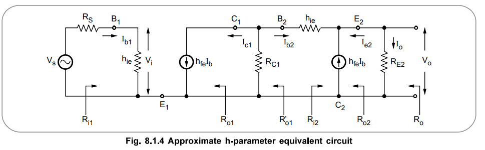
Analysis
of first stage (CE amplifier)
a)
Current gain (A12) = 1 + hfe = 1 + 50 = 51
b)
Input resistance (R12) = hie + (1 + hfe ) RE2
= 2 K + (1 + 50) × 47 × 103 = 241.7 k Ω
3. n-Stage Cascaded Amplifier
•
The gain of the amplifier can be further increased by connecting more number of
stages in cascade, as shown in the Fig. 8.1.7.

Voltage
gain :
•
We have seen that the resultant voltage gain of the multistage amplifier is the
product of voltage gains of the various stages.
Av
= Av1 Av2 … Avn
•
The voltage gain of the kth stage is given as,
Avk
= AikRLk / Rik
where
RLk is the effective load resistance of the kth stage and
Rik is the input impedance of the kth stage.
4. Gain in Decibels
•
In many situations it is found very convenient to compare two powers on a
logarithmic scale rather than on a linear scale. The unit of this logarithmic
scale is called decibel (abbreviated dB). The number N decibels by which a
power P2 exceeds the power Pj is defined by
N
= 10 log P2 / P1 ...(8.1.4)
•
Decibel, dB denotes power ratio. Negative values of number of dB means that the
power P2 is less than the reference power P1 and positive
value of number of dB means that the power P2 is greater than the
reference power P1.
•
For an amplifier, P1 may represent input power, and P2
may represent output power. Both can be given as
P1 = V2i / Ri and
P2 = V2o /
Ro
where
Ri and Ro are the input and output impedances of the amplifier respectively.
Then equation (8.1.4) can be written as,
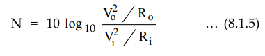
•
If the input and output impedances of the amplifier are equal i.e. Ri
= Ro = R, then equation (8.1.5) simplifies to

Ex.
8.1.2 If the voltage gain of the amplifier is 100, calculate its gain on dB
scale.
Sol.
:
Gain in dB = 20 log 10 100 = 20 × 2 = 40 dB
a.
Gain of Multistage Amplifier in dB
•
The gain of a multistage amplifier can be easily calculated if the gain of the
individual stages are known in dB, as shown below.

•
Thus, the overall voltage gain in dB of a multistage amplifier is the sum of
the decibel voltage gains of the individual stages. It can be given as
AvdB
= AvldB + Av2dB + …+
AvndB … (8-1-8)
Ex.
8.1.3 Two amplifiers having gain 20 dB and 40 dB are cascaded. Find the overall
gain in dB.
AU
: Dec.-09, Marks 2
Sol.
:
Overall gain in dB = 20 + 40 = 60 dB.
b. Advantages of Representation of Gain in Decibels
Logarithmic
scale is preferred over linear scale to represent voltage and power gains
because of the following reasons :
•
In multistage amplifiers, it permits to add individual gains of the stages to
calculate overall gain. (Use of logarithms changes multiplication into an
addition).
•
It allows us to denote, both very small as well as very large quantities of
linear scale by considerably small figures.
•
For example, voltage gain of 0.0000001 can be represented as -140 dB and
voltage gain of 1,00,000 can be represented as 100 dB.
•
Many times output of the amplifier is fed to loudspeakers to produce sound
which is received by the human ear. It is important to note that the ear
responds to the sound intensities on a proportional or logarithmic scale rather
than linear scale. Thus use of dB unit is more appropriate for representation
of amplifier gains.
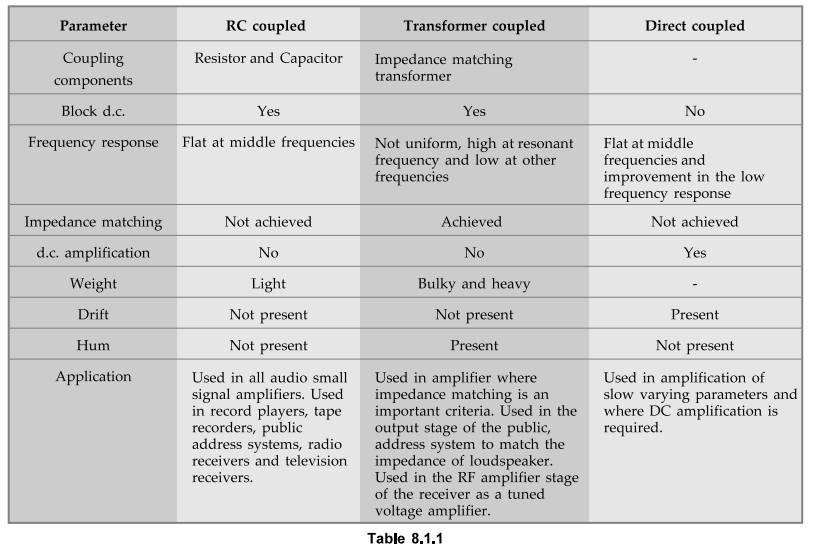
5. Methods of Coupling Multistage Amplifiers
•
In multistage amplifier, the output signal of preceding stage is to be coupled
to the input circuit of succeeding stage. For this interstage coupling,
different types of coupling elements can be employed. These are :
1.
RC coupling
2.
Transformer coupling
3.
Direct coupling
a.
RC Coupling
•
Fig. 8.1.8 shows RC coupled amplifier using transistors. As shown in the Fig.
8.1.8 the output signal of first stage is coupled to the input of the next
stage through coupling capacitor and resistive load at the output terminal of
first stage.

•
The coupling does not affect the quiescent point of the next stage since the
coupling capacitor CC V blocks the d.c. voltage of the first stage from reaching
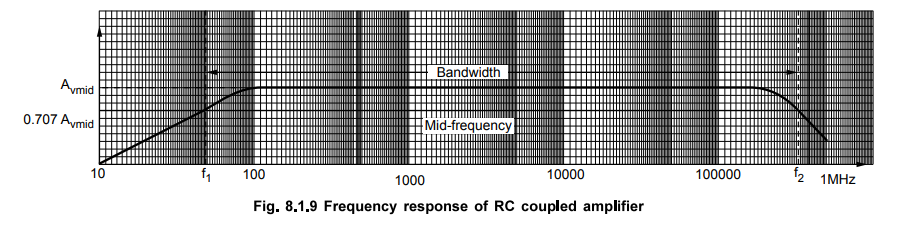
the base of the second stage. The RC network is broadband in nature. Therefore,
it gives a wideband frequency response without peak at any frequency and hence
used to cover a complete AF amplifier bands. However its frequency response
drops off at very low frequencies due to coupling capacitors and also at high
frequencies due to shunt capacitors such as stray capacitance.
•
Fig. 8.1.9 shows the frequency response of RC coupled amplifier.
b.
Transformer Coupling
•
Fig. 8.1.10 shows transformer coupled amplifier using transistors. As shown in
the Fig. 8.1.10 the output signal of first stage is coupled to the input of the
next stage through an impedance matching transformer.

•
This type of coupling is used to match the impedance between output and input
cascaded stage. Usually, it is used to match the larger output resistance of AF
power amplifier to a low impedance load like loudspeaker. As we know,
transformer blocks d.c., providing d.c. isolation between the two stages.
Therefore, transformer coupling does not affect the quiescent point of the next
stage.
•
Frequency response of transformer coupled amplifier is poor in comparison with
that of an RC coupled amplifier. Its leakage inductance and interwinding
capacitances does not allow amplifier to amplify the signals of different
frequencies equally well. Interwinding capacitance of the transformer coupled may
give rise resonance at certain frequency which makes amplifier to give very
high gain at that frequency. By putting shunting capacitors across each winding
of the transformer, we can get resonance at any desired RF frequency. Such
amplifiers are called tuned voltage amplifiers.
•
These provide high gain at the desired of frequency, i.e. they amplify
selective frequencies. For this reason, the transformer-coupled amplifiers are
used in radio and TV receivers for amplifying RF signals.
•
As d.c. resistance of the transformer winding is very low, almost all d.c.
voltage applied by VCC is available at the collector. Due to the
absence of collector resistance it also eliminates unnecessary power loss in
the resistor.
•
Fig. 8.1.11 shows the frequency response of transformer coupled amplifier.

•
Fig. 8.1.13 shows direct coupled amplifier using transistors. As shown in the
Fig. 8.1.13 the output signal of first stage is directly connected to the input
of the next stage. This direct coupling allows the quiescent d.c. collector
current of first stage to pass through base of the next stage, affecting its
biasing conditions.

•
Due to absence of RC components, its low frequency response is good but at
higher frequencies shunting capacitors such as stray capacitances reduce the
gain of the amplifier.
•
The transistor parameters such as VBE and p change with temperature causing the
collector current and voltage to change. Because of direct coupling these
changes appear at the base of the next stage, and hence in the output. Such an
unwanted change in the output is called drift and it is serious problem in the
direct coupled amplifiers.
d.
Comparison between Various Cascading Methods
Electron Devices and Circuits: Unit IV: Multistage and Differential Amplifiers : Tag: : Equivalent circuit, Solved Example Problems - Multistage Amplifiers
Related Topics
Related Subjects

Electron Devices and Circuits
EC3301 3rd Semester EEE Dept | 2021 Regulation | 3rd Semester EEE Dept 2021 Regulation