Electron Devices and Circuits: Unit II: (c) MOSFET
Nonideal Current Voltage Characteristics of MOSFET
• So far, we have seen the ideal current-voltage(drain) characteristics of MOSFET. In practice, the current-voltage characteristics of MOSFET have five nonideal effects. These are : • Finite output resistance • Body effect • Subthreshold conduction • Breakdown effects and • Temperature effects.
Nonideal Current Voltage Characteristics
•
So far, we have seen the ideal current-voltage(drain) characteristics of
MOSFET. In practice, the current-voltage characteristics of MOSFET have five
nonideal effects. These are :
•
Finite output resistance
•
Body effect
•
Subthreshold conduction
•
Breakdown effects and
•
Temperature effects.
1. Finite Output Resistance
•
In ideal case, when a MOSFET is biased in the saturation region, the drain
current, ID is independent of drain-to-source voltage, V Therefore, output
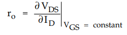
resistance or drain resistance.
ro
= ∂ VDS / ∂ ID | VGS = constant = ∞
•
However, In practice, the ID is slightly dependent on the drain to source
voltage, VDS. This can be observed on ID versus VDSes exists beyond the
saturation point. Refer Fig 4.4.1 (b)
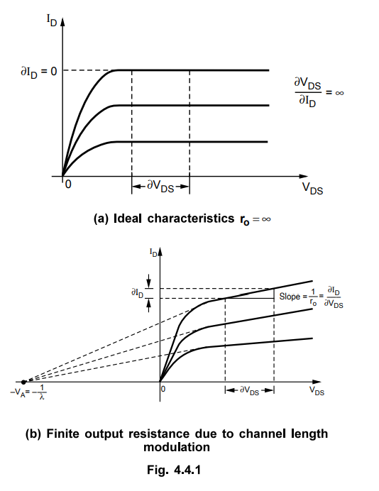
• For VDS > VDS (sat) y ^ie achial point in the channel at which the inversion charge goes to zero moves away from the drain terminal (Refer Fig. 4.3.10 (d)).
•
The effective channel length decreases, and hence the slope exists in the
saturation region of V-I characteristics.
•
This slope of the curve in the saturation region can be described by expressing
the ID versus VDS characteristics in the form, for an n-channel device,
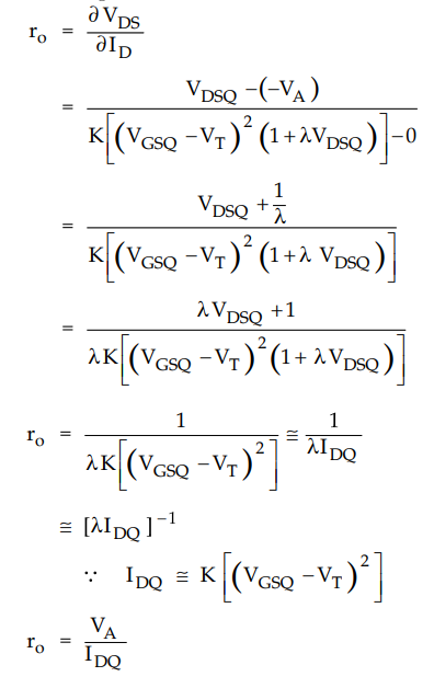
ID
= K[(VGS - VT )2 (1 + λ VDS)] ...(4.4.1)
where
λ is a positive quantity called the channel length modulation parameter.
•
As shown in the exaggerated view of V-I characteristics, the curves can be
extrapolated to get intercept to voltage axis at a point VDS = -VA
•
The voltage VA is usually defined as a positive quantity and is
similar to the early voltage of a bipolar transistor.
•
The parameter λ and VA can be related. From equation (4.4.1) we have
(1+ λVDS) = 0 at the extrapolated point where ID = 0- At
the point, VDS = - VA. Therefore,
1
+ λ (- VA ) = 0
VA
= 1 / λ
•
The output resistance ro due to the channel length modulation is
defined as
•
From equation (4.4.1) we can evaluate the output resistance at the Q point as
Important
Concept
In
practice, ro is not infinite; it has some finite value and it
appears in the small signal equivalent circuit of MOSFET.
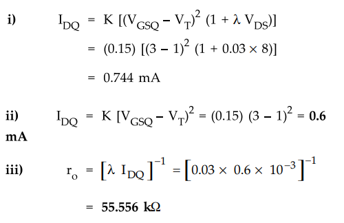
Ex.
4.4.1 The n-channel E-MOSFET has the following parameters : VGSQ = 3V,VT
= 1V, K= 0.15 mA/ V2, X = 0.03 V-1 = 8V
Calculate
: i) Drain current ii) The output resistance.
Sol.
:
Ex.
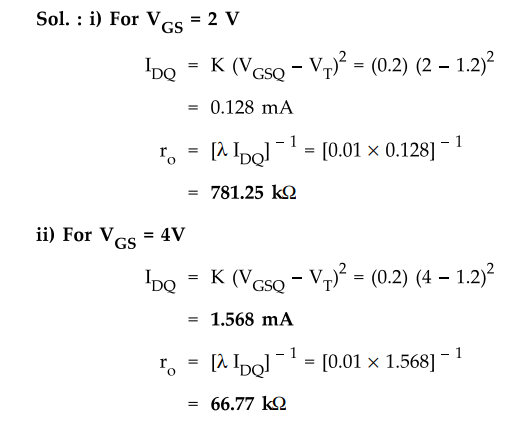
4.4.2 The parameters of n-channel E-MOSFET are K = 0.2mA/V2, X= 0.01
V-1, VT = 1.2 V. Calculate the output resistance for :
i)
VGS = 2 V ii) VGS = 4 V.
Sol.
:
2. Body Effect
•
In integrated circuits the substrate, or body, of all n-channel MOSFETs are
usually common and are connected to the most negative potential in the circuit.
•
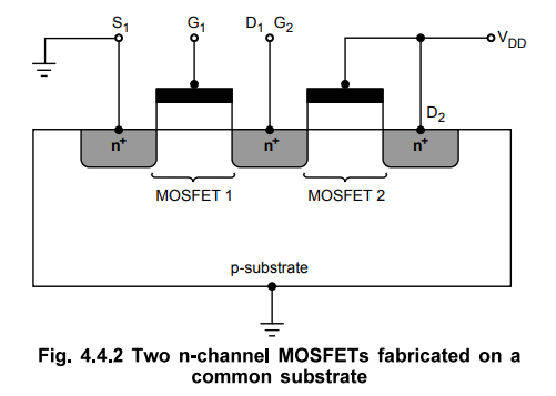
The Fig. 4.4.2 shows the two n-channel MOSFETs in series with a common
p-substrate.
•
The drain of MOSFET1 is common to the source of MOSFET2. When the two MOSFETs
are conducting, there is a nonzero drain-to-source voltage on MOSFET1, which
means that the source of MOSFET2 is not at the same potential as the substrate.
•
As a result, there exists zero or reverse bias voltage across the source
substrate p-n junction of MOSFET2. The change in this reverse bias voltage
changes the threshold voltage. This is known as body effect. The same effect
also exists in p-channel devices.
•
Consider the n-channel device shown in Fig. 4.4.3. To maintain a zero or
reverse biased source substrate p-n junction, VSB must be greater than or equal
to zero. The threshold voltage for this condition is given by
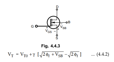
where,
VTO • Threshold voltage for VSB = 0
•
ɤ : Bulk threshold or body effect parameter. It is related to device properties
and is typically of the order of 0.5 V1/2.
•
ϕ f : Semiconductor parameter, typically of the order of 0.35 V.
•
It is a function of semiconductor doping.
Important
Concepts
1.
The equation says that VT increases due to body effect.
2.
The body effect can cause a degradation in circuit performance because of the
changing threshold voltage.
3. Subthreshold Condition
•
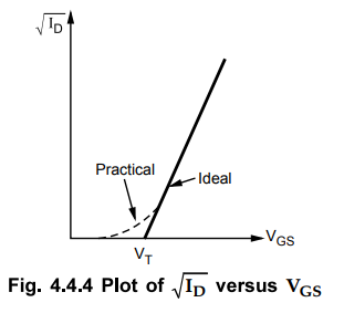
The drain current, ID in the ideal V-I characteristic is given by
ID
= K (VGS - VT )2
•
Taking square roots on both sides we have,
√ID
= √K (VGS - VT )
•
The above relation is represented in Fig. 4.4.4. The ideal curve in the figure,
says that √ID is a linear function of VGS
•
However, in practice, when VGS slightly less than VT, the
drain current, ID is not zero. This current is called the
subthreshold current.
•
This effect may not be significant for a single device, but if hundreds or
thousands of devices on an integrated circuit are biased just slightly below
the threshold voltage, the power supply current will not be zero but may contribute
to significant power dissipation in the integrated circuit.
4. Breakdown Effects
•
There are three different breakdown effects which may occur in a MOSFET. These
are
•
Breakdown due to avalanche multiplication.
•
Breakdown due to punch-through effect.
•
Breakdown due to near-avalanche or snapback.
•
Breakdown due to static charge.
1.
Breakdown due to avalanche multiplication
•
When applied drain voltage is too high, the drain-to-substrate p-n junction may
breakdown due to avalanche multiplication.
•
This breakdown is same as reverse biased p-n junction breakdown.
2.
Breakdown due to punch-through effect
•
Punch-through occurs when the drain voltage is large enough for the depletion
region around the drain to extend completely through the channel to the source
terminal.
•
This effect also causes the drain current to increase rapidly with only a small
increase in drain voltage.
•
The punch through breakdown mechanism may become significant for smaller size
devices.
3.
Breakdown due to near-avalanche or snapback
•
The near-avalanche or snapback breakdown occurs due to second-order effects
within the MOSFET, such as parasitic action or excess electric field in the
oxide.
4.
Breakdown due to static charge
•
The input impedance of MOSFET is very high. Because of this a small amount of
static charge accumulating on the gate can cause the breakdown voltage to be
exceeded.
•
To prevent the accumulation of static charge on the gate, a gate protective
device, such as a reverse-biased diode is usually included at the input of a
MOSFET.
5. Temperature Effects
•
Due to change in temperature, there is a change in threshold voltage, VT
and condition parameter K.
•
The magnitude of the threshold voltage decreases with temperature, which means
that the drain current increases with temperature at a given VGS-
•
The condition parameter K is a direct function of the inversion carrier
mobility, which decreases as the temperature increases. This causes reduction
in drain current.
•
Since the temperature dependance of mobility is larger than that of the
threshold voltage, the net effect of increasing temperature is a decrease in
drain current at a given VGS-
•
This particular result provides temperature stability for MOSFETs and prevent
them from thermal runaway.
Review Questions
1. Explain any three non-ideal current voltage characteristics
of MOSFET transistor.
2. Explain the following non-ideal current voltage
characteristics of MOSFET:
i) Finite output resistance
ii) Body effect
iii) Subthreshold conduction.
3. State true or false :
i) MOSFET does not suffer from thermal runaway.
ii) MOS devices are subject to damage from electrostatic
discharge.
iii) Channel-length modulation makes the output resistance in
saturation finite.
iv) MOSFET offers extremely high input resistance.
4. Explain the following non-ideal characteristics of MOSFET :
i) Breakdown effect
ii) Temperature effect
iii) Subthreshold conduction.
5. Define the following non-ideal parameters of MOSFET :
i) Body effect ii) Subthreshold conduction.
6. Explain the following non-ideal 1-V characteristics
ofE-MOSFET:
i) Finite output resistance ii) Body effect iii) Temperature
effect.
7. What are the various non-ideal effects in MOSFETs ? Explain
any two in detail.
8. Define drain resistance.
Electron Devices and Circuits: Unit II: (c) MOSFET : Tag: : - Nonideal Current Voltage Characteristics of MOSFET
Related Topics
Related Subjects

Electron Devices and Circuits
EC3301 3rd Semester EEE Dept | 2021 Regulation | 3rd Semester EEE Dept 2021 Regulation