Linear Integrated Circuits: Unit III: Applications of Op-amp
Op-amp as a comparator
When two inputs are applied to the open loop op-amp then it compares the two inputs. Depending upon the comparison, it produces output voltage which is either positive saturation voltage (+ Vsat) or negative saturation voltage (- Vsat).
op-amp as a comparator
The
op-amp in open loop configuration can be used as a basic comparator. When two
inputs are applied to the open loop op-amp then it compares the two inputs.
Depending upon the comparison, it produces output voltage which is either
positive saturation voltage (+ Vsat) or negative saturation voltage
(- Vsat).
A
comparator is a circuit which compares a signal voltage applied at one input of
an op-amp with a known reference voltage at the other input and produce either
a high or a low output voltage, depending on which input is higher. As
comparator output has two voltage levels, either high or low, it is not
linearly proportional to input voltage.
There
are two types of comparator circuits which are,
1.
Non-inverting comparator 2. Inverting comparator.
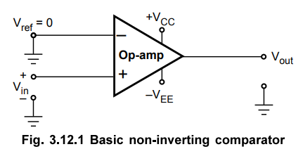
1. Basic Non-inverting Comparator
In
this comparator, the input voltage is applied to the non-inverting terminal and
no reference voltage is applied to other terminal. So inverting terminal is
grounded. The input voltage is denoted as Vin while the voltage
applied to other terminal with which is compared is denoted as Vref.
In the basic comparator, Vref = 0 V. The basic non-inverting
comparator is shown in the Fig. 3.12.1.
In
the non-inverting comparator, if Fig. 3.12.1 Basic non-inverting comparator is
greater than Vref then output is + Vsat i.e. almost equal to + VCC.
While if Vin is less than Vref then output is - Vsat
i.e. almost equal to - VEE.
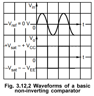
Thus
for Fig. 3.12.1, as Vref = 0 V when Vin is positive then
Vo = + Vsat ≈ + VCC while when is negative
then Vo = - Vsat ≈- VEE. This is because, as
open loop gain op-amp (AOL) is very very high even for very small
the op-amp output saturates.
Thus
the two possible output levels of the comparator are + Vsat and - Vsat,
indicating whether the input voltage is greater than or less than the reference
voltage. Such type of the comparator, in which the operation is at saturation
level is known as saturating type of comparator. Assuming symmetrical
conditions, the two possible output levels of the saturating type comparator
are + Vsat and - Vsat.
Note
that no feedback is applied to the op-amp and it is operated in open loop
conditions, because of which the op-amp is operating in saturating conditions.
The
input and output waveforms for a basic non-inverting comparator, for sinusoidal
input are shown in the Fig. 3.12.2.
The
op-amp differential voltage gain AOL is very large. So when
inverting input is grounded, very small input voltage in the range of microvolt
is enough to saturate the op-amp. The ±Vsat , the saturation voltage
levels of op-amp are mentioned in the data sheet. Hence knowing Vsat
and differential non-inverting comparator voltage gain A, we can determine the
minimum input voltage level required to saturate op-amp as,
Vin
(min) = Vsat / AOL for
saturation
Now
the transfer characteristics is the graph of and Vout. As AOL is very large
hence for very very small positive or negative V^, the output saturates. Hence
at = 0, the transfer characteristics is almost a straight line as shown in the
Fig. 3.12.3 (a). For example, for 741 C op-amp, AOL is 100,000 while
± Vsat levels are ± 13.5 V for supply of ±15 V.
Vin
= Vsat / AOL = ± 13.5 / 100000 = ± 135 µV
Thus
for + 135 µV of Vin, output saturates to + Vsat while
-135 µV of is enough to saturate output at - Vsat. Hence region -135
µV to + 135 µV of the graph of and Vout is linear. But this range is so small
that near Vin = 0 practically we get a straight line transfer
characteristics.
The
Fig. 3.12.3 (a) and (b) shows the ideal and practical transfer characteristics
of a basic non-inverting comparator.
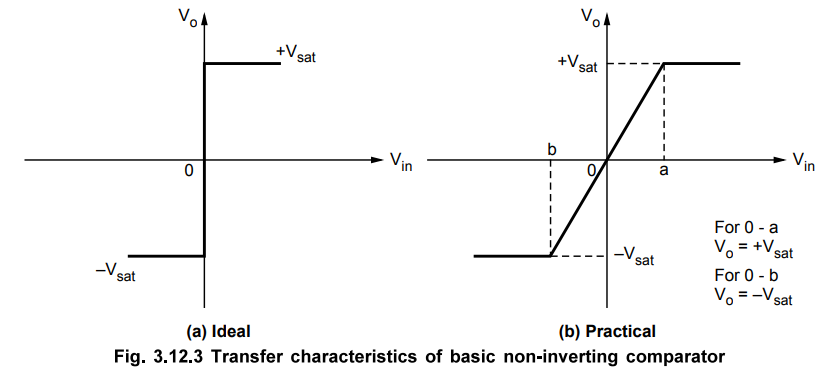
The
point at which the transfer characteristics is straight line is called a trip
point. The trip point is the input voltage at which the output changes its states
from low to high or high to low. In the basic comparator this trip point is
zero as at = 0, the output changes its states.
Key
Point So we can say that when Vin is greater than trip
point, the output is high while if Vin is less than the trip point the ouput is
low.
As
this change over occurs at = 0, the basic comparator can be used to detect
occurrence of zero in the input voltage. Hence this circuit is called zero
crossing detector. But in practice it is possible to change the trip point from
zero to other voltage. This is achieved by some modifications in the basic
comparator circuit.
Moving
a Trip Point
By
application of a reference voltage to the inverting input rather than grounding
it, the trip point can be moved.
The
Fig. 3.12.4 shows the application of reference voltage to the inverting input
of a basic comparator using a potential divider consisting of resistors R1
and R2.
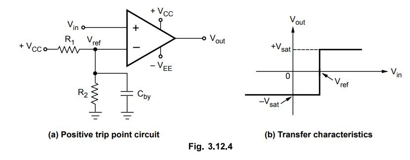
The
reference voltage Vref is derived using supply + VCC and
potential divider R1 and R2. Mathematically Vref
is expressed as,
Vref
= (+VCC / R1
+ R2) R2
Now
as long as input voltage is less than Vref, the output is low i.e. -
Vsat. When becomes slightly greater than Vref, the op-amp
output becomes high i.e. + Vsat. Thus the trip point is moved from =
0 to = Vref due to reference voltage applied to the inverting input
terminal.
A
bypass capacitor is used on the inverting input to reduce the amount of power
supply ripple and noise appearing at the inverting input of op-amp. For
effective bypassing of ripple and noise, the critical frequency of the bypass
circuit must be much lower than the ripple frequency of power supply.
The
transfer characteristics of such a comparator is shown in the Fig. 3.12.4 (b)
which indicates positive trip point. Such a comparator is also called a limit
detector as it detects the particular positive level of input beyond which output
goes high. The resistances R1 and R2 can be used to set
the trip point anywhere between 0 and + VCC.
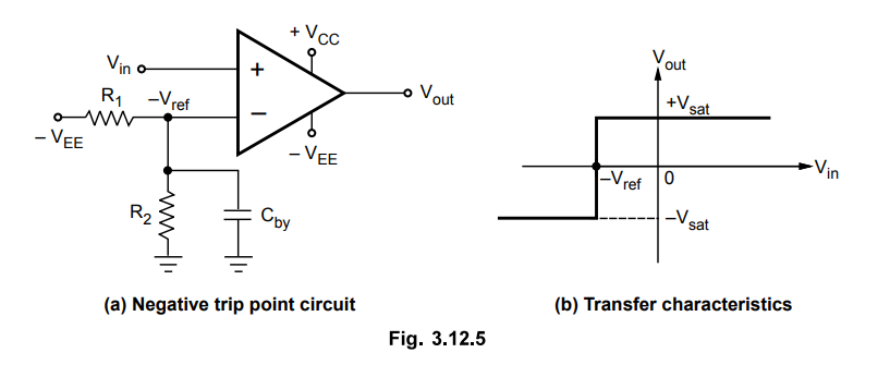
It
is possible to obtain a negative trip point by providing a negative reference
voltage to the inverting input. This is achieved by using a supply - VEE
to the potential divider of R1 and R2.
Vref
= (-R2 / R1 + R2) VEE
This
is shown in the Fig. 3.12.5 (a). When Vin is positive than -Vref
, error voltage is positive which drives op-amp into positive saturation. When
is more negative than -Vref, error voltage is negative which drives
op-amp into negative saturation producing low output. The transfer
characteristics is shown in the Fig. 3.12.5 (b).
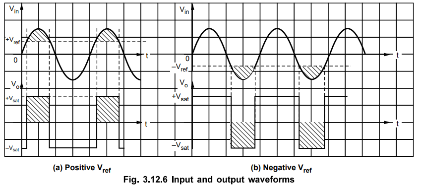
The
Fig. 3.12.6 (a) shows input and output waveforms with positive reference
voltage while the Fig. 3.12.6 (b) shows input and output waveforms with
negative reference voltage.
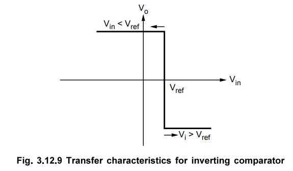
2. Inverting Comparator
The
Fig. 3.12.7 shows inverting comparator in which the reference voltage Vref
is applied to the non-inverting (+) input and signal voltage (Vin)
is applied to the inverting (-) input of the op-amp. The Vref can be
set using a battery and potential divider as discussed earlier for
non-inverting comparator.
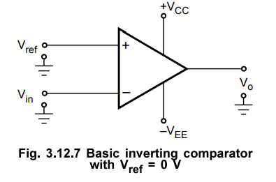
When
Vin is less than Vref, the output voltage Vo
is at + Vsat (= +VCC) because the voltage at the
inverting input (-) is less than that at the non-inverting (+) input. On the
other hand, when Vin is greater than Vref, the non-inverting
(+) input becomes negative with respect to the inverting (-) input and Vo goes
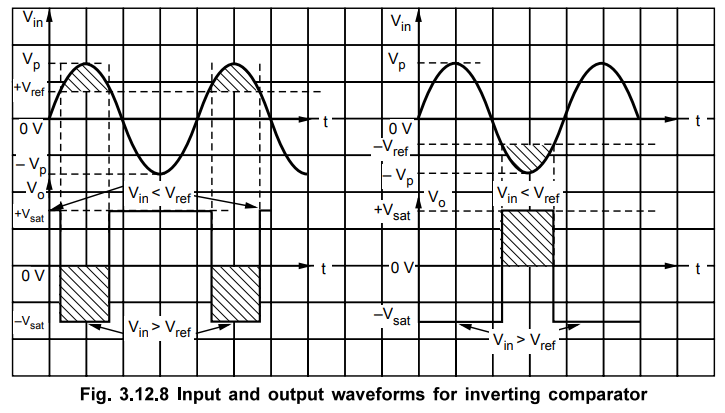
to -Vsat (≅
-VEE). The Fig. 3.12.8 shows the input and output waveforms for
inverting comparator.
Transfer
characteristics for inverting comparator with +Vref is shown in the Fig.
3.12.9.
3. Practical Comparator
The
Fig. 3.12.10 shows practical comparator circuit. It consists of protective diodes and potentiometer to adjust the
reference voltage.
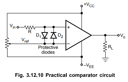
As
shown in Fig. 3.2.10 diode D1 and diode D2 are connected
to protect the op-amp from damage due to excessive input voltage Vin.
Because of these diodes, the difference input voltage Vid is always
less than 0.7 V or -0.7 V. In case of excess input voltage, the difference
input voltage Vid °f op-amp is clamped to either 0.7 V or -0.7 V due to the
forward biasing of one of the diodes. Hence, these diodes are also called as
damp diodes. Some op-amps have built-in input protection circuitry; they don't
require external clamp diodes. The resistance R in series with Vin
is used to limit the current through D1 and D2- The
potentiometer acts as a voltage divider and allows reference voltage to set any
value between + VCC to -VEE Some of the applications of
comparator are zero crossing detector, level detector, window detector, duty
cycle controller and pulse generator.
4. Applications of Comparator
The
various applications of comparator are,
1.
Zero crossing detector 2. Level detector 3. Window detector 4. Duty cycle
controller 5. Pulse generator 6. Time marker generator .
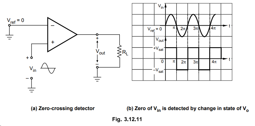
a.
Zero Crossing Detector
The
basic comparator can be used as a zero crossing detector. It answers the
questions: Is the input signal greater than or less than zero ? A typical
circuit for such a detector is shown in Fig. 3.12.11 (a). It is a noninverting
comparator circuit with Vref = 0V.
During
the positive half cycle, the input voltage is positive i.e. above the reference
voltage. Hence the output voltage is Vsat+. During
negative half cycle, the input voltage Vin is negative, i.e. below the
reference voltage. The output voltage is then Vsat .Thus the output
voltage switches between Vsat+ and Vsat - whenever the
input signal crosses the zero level. This is illustrated in Fig. 3.12.11 (b).
Looking
at the waveform shown in Fig. 3.12.11 (b) we realize that zero crossing
detector can be used as sine to square wave converter.
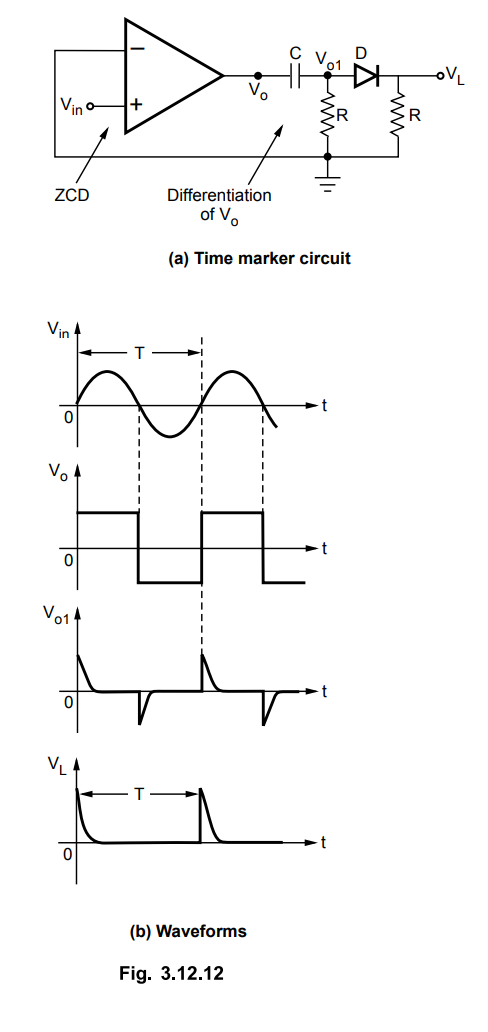
b.
Time Marker Generator
In this circuit, the output of the zero crossing detector is differentiated using RC circuit. This produces a train of positive and negative pulses denoted as Vo1 in the Fig. 3.12.12 (a). Then the negative pulses can be eliminated using a diode. Thus output is a train of positive pulses separated by T as shown in the Fig. 3.12.12 (b). Such signal can be used as triggering signal for other devices such as monostable multivibrator, SCR etc.
Review Question
1. Discuss the
comparator using op-amp and its applications.
Linear Integrated Circuits: Unit III: Applications of Op-amp : Tag: : - Op-amp as a comparator
Related Topics
Related Subjects

Linear Integrated Circuits
EE3402 Lic Operational Amplifiers 4th Semester EEE Dept | 2021 Regulation | 4th Semester EEE Dept 2021 Regulation