Linear Integrated Circuits: Unit II: Characteristics of Op-amp
Op-amp Differentiator
Working Principle, Waveform, Circuit Diagram, Applications, Solved Example Problems | Operational amplifier
The circuit which produces the differentiation of the input voltage at its output is called differentiator. The differentiator circuit which does not use any active device is called passive differentiator.
Differentiator
The
circuit which produces the differentiation of the input voltage at its output
is called differentiator. The differentiator circuit which does not use any
active device is called passive differentiator. While the differentiator using
an active device like op-amp is called an active differentiator. Let us discuss
first the operation of ideal active op-amp differentiator circuit.
1. Ideal Active Op-amp Differentiator
The
active differentiator circuit can be obtained by exchanging the positions of R
and C in the basic active integrator circuit. The op-amp differentiator circuit
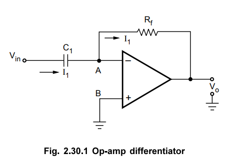
is shown in the Fig. 2.30.1.
The
active differentiator circuit can be obtained by exchanging the positions of R
and C in the basic active integrator circuit. The op-amp differentiator circuit
is shown in the Fig. 2.30.1.
The
node B is grounded. The node A is also at the ground potential hence VA
= 0.
As input current of op-amp is zero, entire current I flows through the resistance Rf.
From the input side we can write,
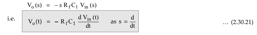
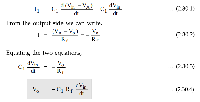 The
equation shows that the output is C1Rf times the
differentiation of the input and product C1Rf is called
time constant of the differentiator.
The
equation shows that the output is C1Rf times the
differentiation of the input and product C1Rf is called
time constant of the differentiator.
The
negative sign indicates that there is a phase shift of 180° between input and
output. The main advantage of such an active differentiator is the small time
constant required for differentiation.
By
Miller's theorem, the effective resistance between input node A and ground
becomes Rf / 1 + Av ≈ Rf / Av where
Av is the gain of the op-amp which is very large. Hence effective Rf
becomes very very small and hence the condition Rf C1
<< T gets satisfied at all the frequencies.
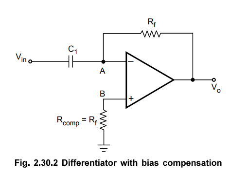
In
practice a resistance Rcomp = Rf is connected to the non-inverting terminal to
provide the bias compensation. This is shown in the Fig. 2.30.2.
2. Input and Output Waveforms
Let
us study the output waveforms, for various input signals.
For
simplicity of understanding, assume that the values of Rf and C1
are selected to have time constant (RfC1) as unity.
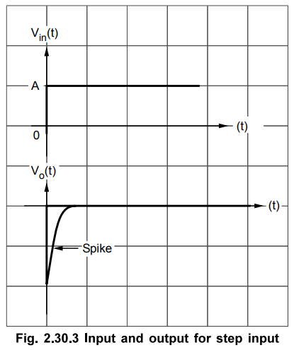
i) Step input signal
Let
the input waveform is of step type with a magnitude of A units. Mathematically
it is expressed as,
Vin
(t) = A for t ≥ 0 ... (2.30.5)
Now
mathematically, the output of the differentiator must be,
Vo
(t) = - dVin / dt = - d(A) / dt = 0 …. (2.30.6)
This
is because A is constant.
Actually
the step input takes a finite time to rise from 0 to A volts.
Due to this finite time, the differentiator output is not zero but appears in the form of a spike at t = 0.
As
the circuit acts as an inverting differentiator, the negative going spike or
impulse appears at t = 0 and after that output remains zero.
Both
input and output waveforms of the differentiator with a step input, are shown
in the Fig. 2.30.3.
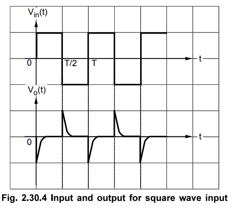
ii)
Square wave input signal
Input
and output for square wave input
The
square wave is made of steps i.e. step of A volts from t = 0 to t = T/2, while
a step of -A volts from t = T/2tot = T and so on.
Mathematically
it can be expressed as,
Vin
(t) = A 0 < t < T/2
=
- A T/2 < t < T … (2.30.7)
The
differentiator behaves similar to its behaviour to step input.
For
positive going impulse, the output shows negative going impulse and for
negative going input, the output shows positive going impulse.
Hence
the total output for the square wave input is in the form of train of impulses
or spikes.
The input and output waveforms are shown in the Fig. 2.30.4
iii)
Sine wave input
Let
the input waveform be purely
sinusoidal
with a frequency of ω rad/sec. Mathematically it can be expressed as,
Vin(t) = Vm sin ωt …. (2.30.8)
where
Vm is the amplitude of the sine wave and T is the period of the
waveform. Let us find out the expression for the output.
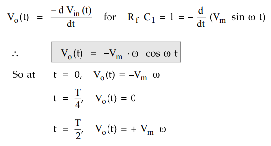
and
so on.
Thus
the output of the differentiator is a cosine waveform, for a sine wave input.
The input and output waveform is shown in the Fig. 2.30.5.

3. Disadvantages of an Ideal Differentiator
The
gain of the differentiator increases as frequency increases. Thus at some high
frequency, the differentiator may become unstable and break into the
oscillations. There is possibility that op-amp may go into the saturation.
Also
the input impedance Xc1= (1 /2π f C1) decreases as
frequency increases. This makes the circuit very much sensitive to the noise.
Thus when such noise gets amplified due to high gain at high frequency, noise
may completely override the differentiated output.
Hence
the differentiator circuit suffers from the limitations on its stability and
noise problems, at high frequencies. These problems can be corrected using some
additional parameters in the basic differentiator circuit. Such a
differentiator circuit is called
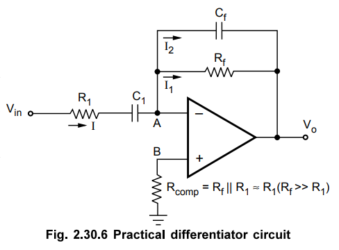
4. Practical Differentiator
The
noise and stability at high frequency can be corrected, in the practical
differentiator circuit using the
resistance R1 in series with C1 and the capacitor Cf in
parallel with resistance Rf.
The
circuit is shown in the Fig. 2.30.6. The resistance Rcomp is used
for bias compensation.
5. The Analysis of the Practical Differentiator
As
the input current of op-amp is zero, there is no current input at node B. Hence
it is at the ground potential. From the concept of the virtual ground, node A
is also at the ground potential and hence VB = VA = 0 V.
For
the current I, we can write
I
= Vin -VA / Z1 = Vin / Z1 …. (2.30.10)
where
Z1 = R1 in series with C1
So
in Laplace domain we can write,
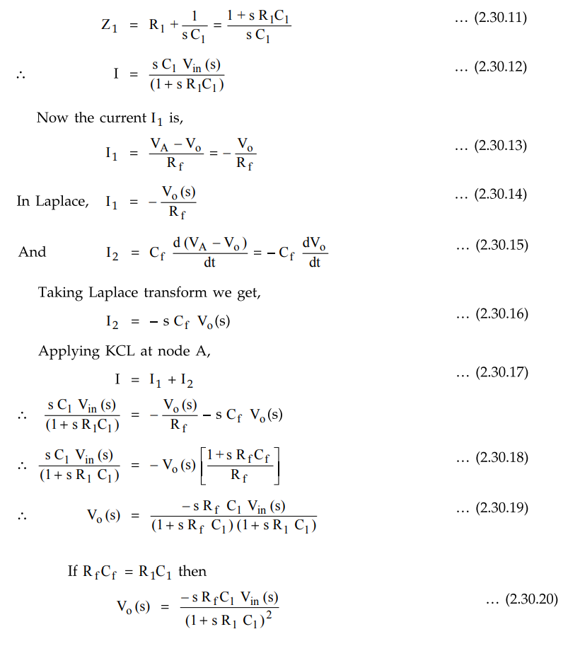
The
time constant RfC1 is much greater than RfC1
or RfCf and
hence the equation (2.30.20) reduces to,
Thus
the output voltage is the RfC 1 times the differentiation of the input.
It
may be noted that though RfC1 is much larger than RfCf
or R1C1 it
is less than or equal to the time period T of the input, for the true
differentiation.
RfC1
≤ T
….. (2.30.22)
6. Frequency Response of Practical Differentiator
To
determine the frequency response, let us obtain the expression for the gain of
the practical differentiator interms of the frequency.
From
the equation (2.30.20) we can write,
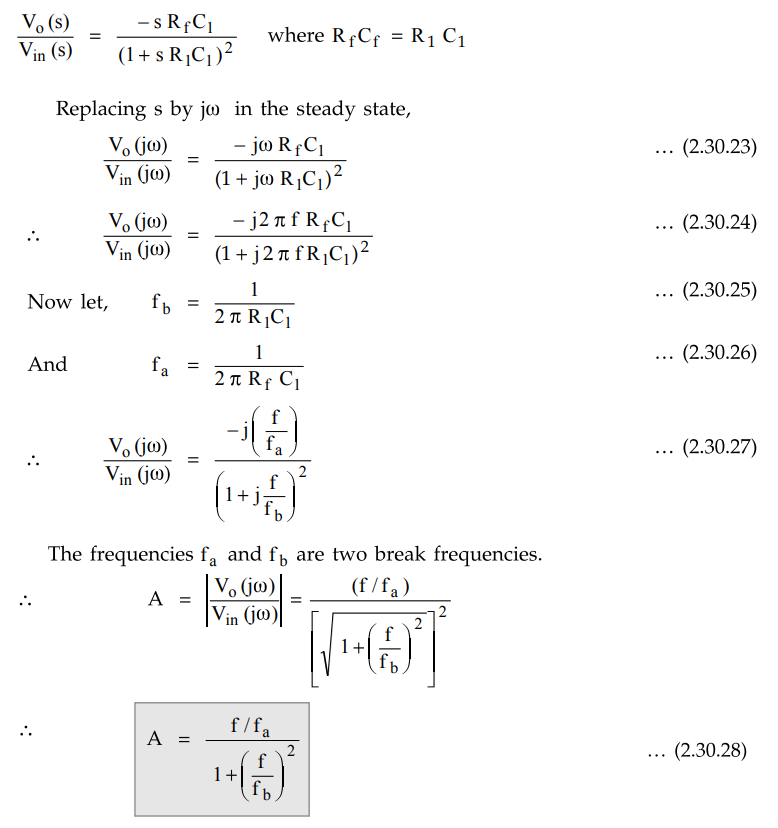
Now
as RfC1 is much larger than R1C1 we
can write
fa
< fb ... (2.30.29)
Hence
as frequency increases, the gain increases till f = fb at a rate of
+20 dB/decade. However after f = fb the gain decreases at a rate of
20 dB/decade. This 40 dB/decade change at f = fb occurs due to the
combination of R1C1 and RfCf.
So
for RfC1 << T, the true differentiation results.
The
frequency response is shown in the Fig. 2.30.7. Refer Fig. 2.30.7.
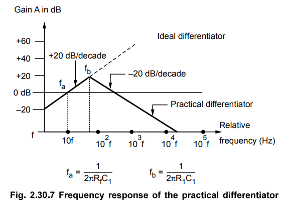
Key Point It can be
observed from the frequency response that the gain reduces as frequency
increases greater than fb- Hence the problem of instability at high frequency
gets eliminated.
Also
the combination of RiCi and RfCf help to reduce effectively the impact of high
frequency noise and offsets.
It
is important to remember that if fc is the Unity Gain Bandwidth (UGB) then the
values of fa and fb must be selected in such a way that,
Fa
< fb < fc …..
(2.30.30)
where
fc is UGB of op-amp in the open loop configuration.
7. Steps to Design Practical Differentiator
By
using following steps, a good practical differentiator can be designed :
i)
Choose fa as the highest frequency of the input signal.
ii)
Choose C1 to be less than 1 µF and calculate the value of Rf.
iii)
Choose fb as 10 times fa which ensures that fa <
fb
iv)
Finally calculate the values of R1 and Cf from the
expression R1C1 = RfCf.
v)
The Rcomp can be selected as R1 || Rf but
practically it is almost equal to R1.
8. Applications of Practical Differentiator
The
practical differentiator circuits are most commonly used in :
i)
In the wave shaping circuits to detect the high frequency components in the
input signal.
ii)
As a rate-of-change detector in the FM demodulators.
The
differentiator circuit is avoided in the analog computers.
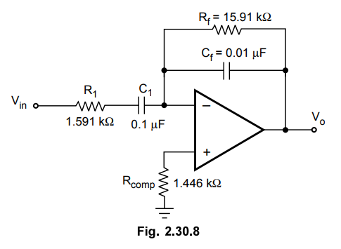
Example
2.30.1 Design a practical differentiator circuit that
will differentiate an input signal with the fmax = 100 Hz.
April-10,
Dec.-14, Marks 8
Solution
: Refer to the
steps for design.
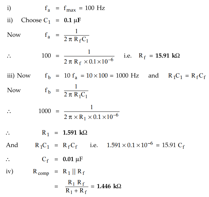
But
generally Rcomp is selected equal to R1. The designed differentiator circuit is
shown in the Fig. 2.30.8.
The
frequency response is as shown in the Fig. 2.30.7
Review Questions
1. What are the
limitations of an ordinary differentiator? Draw the circuit of practical
differentiator and explain.
May-08, Dec.-15, Marks
12
2. Explain the
application of op-amp as a differentiator.
May-10,11,16,
Dec.-11,12, Marks 4
3. Derive an
expression for the output of a practical differentiator.
Dec.-12, Marks 6
4. Explain the
application of Op-Amp as differentiator.
May-16, Marks 8
Linear Integrated Circuits: Unit II: Characteristics of Op-amp : Tag: : Working Principle, Waveform, Circuit Diagram, Applications, Solved Example Problems | Operational amplifier - Op-amp Differentiator
Related Topics
Related Subjects

Linear Integrated Circuits
EE3402 Lic Operational Amplifiers 4th Semester EEE Dept | 2021 Regulation | 4th Semester EEE Dept 2021 Regulation