Linear Integrated Circuits: Unit II: Characteristics of Op-amp
Op-amp Integrator
Working Principle, Waveform, Circuit Diagram, Applications, Solved Example Problems | Operational amplifier
The integrator circuit can be obtained without using active devices like op-amp, transistors etc. In such a case an integrator is called passive integrator.
Integrator
May-03,04,07,08,09,10,11,12,15,
Dec.-06,08,09,ll,14
In
an integrator circuit, the output voltage is the integration of the input
voltage. The integrator circuit can be obtained without using active devices
like op-amp, transistors etc. In such a case an integrator is called passive
integrator. While an integrator using an active devices like op-amp is called
active integrator. In this section, we will discuss the operation of active
op-amp integrator circuit.
1. Ideal Active Op-amp Integrator
Consider
the op-amp integrator circuit as shown in the Fig. 2.29.1.
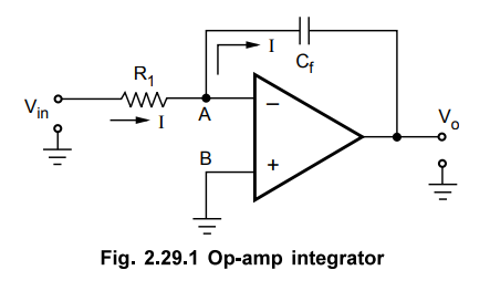
The
node B is grounded. The node A is also at the ground potential from the concept
of virtual ground.
VA
= 0 = VB
As
input current of op-amp is zero, the entire current I flowing through R1,
also flows through Cf, as shown in the Fig. 2.29.1.
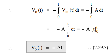
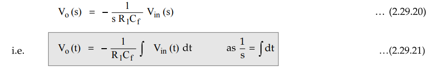
where
Vo (0) is the constant of integration, indicating the initial output
Voltage.
The
equation (2.29.5) shows that the output is - 1/ R1 Cf
times the integral of input and R1 Cf is called time
constant of the integrator.
The
negative sign indicates that there is a phase shift of 180° between input and output.
The main advantage of such an active integrator is the large time constant. By
Miller's theorem the effective capacitance between input terminal A and the
ground becomes Cf (1-Av ) where Av is the gain
of the op-amp which is very large. Due to such large effective capacitance,
time constant is very large and thus a perfect integration results due to such
circuit.
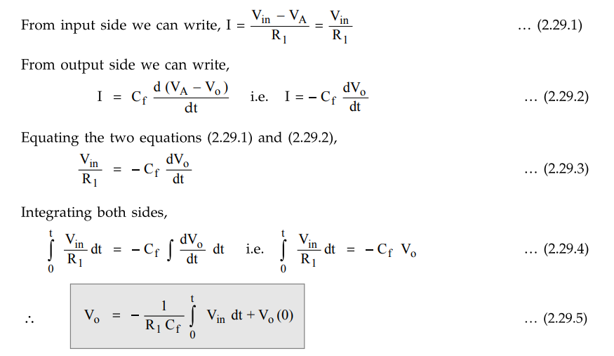
Sometimes
a resistance Rcomp = R1 is connected to the non-inverting
terminal to provide the bias compensation. This is shown in the Fig. 2.29.2.
As
the input current of op-amp is zero, the node B is still can be treated at
ground potential in this circuit.
Key Point Hence the above
analysis is equally applicable to the integrator circuit with bias
compensation. And the output is the perfect integration of the input.
2. Input and Output Waveforms
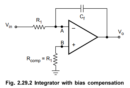
Let
us see the output waveforms, for various input signals. For simplicity of
understanding, assume that the time constant
R1Cf = 1 and the initial voltage Vo (0)
= 0V
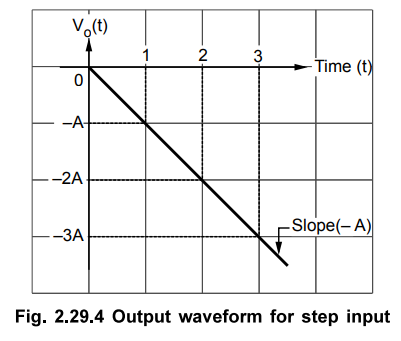
i)
Step input signal
Let
the input waveform is of step type, with a magnitude of A units as shown in the
Fig. 2.29.3
Mathematically
the step input can be expressed as,
Vin
(t) = A for t ≥ 0
And = 0 for t ≤ 0
From
equation (2.29.5), with R1Cf = 1 and Vo(0) = 0,
We
can write,
Thus
output waveform is a straight line with a slope of -A where A is magnitude of
the step input. The output waveform is shown in the Fig. 2.29.4.
ii)
Square wave input signal
Let
the input waveform is a square wave as shown in the Fig. 2.29.5
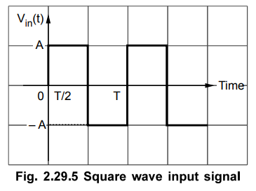
It
can be observed that the square wave is made up of steps i.e. a step of A
between time period of 0 to T/2 while a step of - A units between a time period
of T/2 to T and so on.
Mathematically
it can be expressed as,
Vin(t)=
A, 0 < t < T/2 ….. (2.29.8)
=
- A, T/2 < t < T
This
is the expression for the input signal for one period.
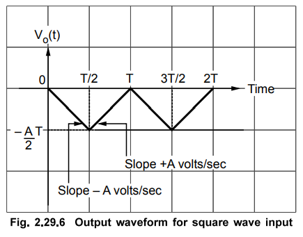
As
discussed earlier, the output for step input is a straight line with a slope of
-A. So for the period 0 to T/2 output will be straight line with slope - A.
From t = T/2 till t = T, the slope of the straight line will become - (-A) i.e.
+ A.
So
the output can be expressed Fig. 2.29.6 Output waveform for square wave input
mathematically for one period as,
Vo(t)=
- A t 0 < t < T/2
=
+ A t T/2 < t < T ….. (2.29.9)
The
output waveform is shown in the Fig. 2.29.6.
iii)
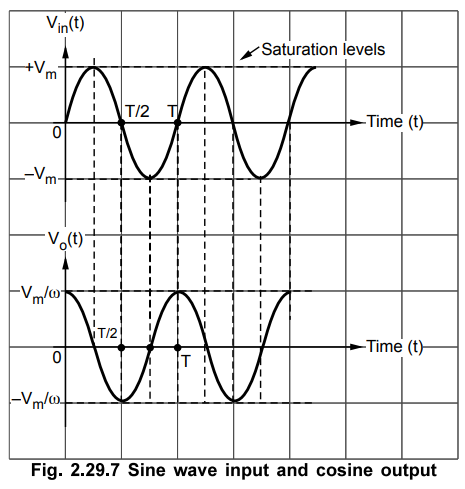
Sine wave input signal
Let
the input waveform is purely sinusoidal with a frequency of co rad/sec.
Mathematically it can be expressed as,
Vin
(t) = Vm Sin ω t ... (2.29.10)
where
Vm is the amplitude of the sine wave and T be the period of the
waveform.
To
find the output waveform, use the equation (2.29.5) with R1Cf
= 1 and Vo(0) = 0 V.
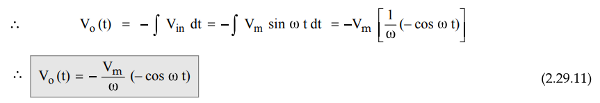
Thus
it can be seen that the output of an integrator is a cosine waveform for a
input. Due to inverting integrator, the output waveform is as shown in the Fig.
2.29.7.
3. Errors in an Ideal Integrator
The
operation amplifier has input offset voltage (Vios) and the input bias
current (Ib)- In the absence of input voltage or at zero frequency (d.c.),
op-amp gain is very high. The input offset voltage gets amplified and appears
at the output as an error voltage. The bias current also results in a capacitor
charging current and adds its effect in an output error voltage.
The
two components, due to high d.c. gain of op-amp cause output to ramp up or
down, depending upon the polarities of offset voltage and/or bias current.
After some time, output of op-amp may achieve its saturation level. Hence there
is a possibility of op-amp saturation due to such an error voltage and it is
very difficult to pull op-amp out of saturation. Thus the output of an ideal
integrator in the absence of input signal is likely to be offset towards the positive
or negative saturation levels.
In
the presence of the input signal also, the two components namely offset voltage
and bias current, contribute an error voltage at the output. Thus it is not
possible to get a true integration of the input signal at the output. Output
waveform may be distorted due to such an error voltage.
Another
limitation of an ideal integrator is its bandwidth, which is very small. Hence
an ideal integrator can be used for a very small frequency range of the input
only.
Due
to all these limitations, an ideal integrator is not used in practice. Some
additional components are used along with the basic integrator circuit to reduce
the effect of an error voltage, in practice. Such an integrator is called
Practical Integrator Circuit.
4. Practical Integrator
The
limitations of an ideal integrator can be minimized in the practical integrator
circuit, which uses a resistance Rf in parallel with the capacitor Cf.
The
practical integrator circuit is shown in the Fig. 2.29.8.
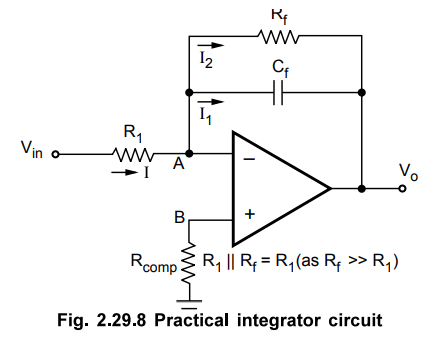
The
resistance Rcomp is also used to overcome the errors due to the bias
current.
The
resistance Rf reduces the low frequency gain of the op-amp.
5. The Analysis of Practical Integrator
As
the input current of op-amp is zero, the node B is still at ground potential.
Hence the node A is also at the ground potential from the concept of virtual
ground.
So
VA = 0.
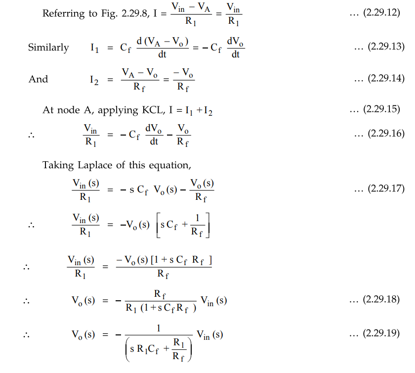
When
Rf is very large then R1/Rf can be neglected
and hence circuit behaves like an ideal integrator as,
6. Frequency Response of Practical Integrator
To
determine the frequency response, let us obtain the expression for the gain of
the practical integrator interms of the frequency.
From
the equation (2.29.18) we can write,
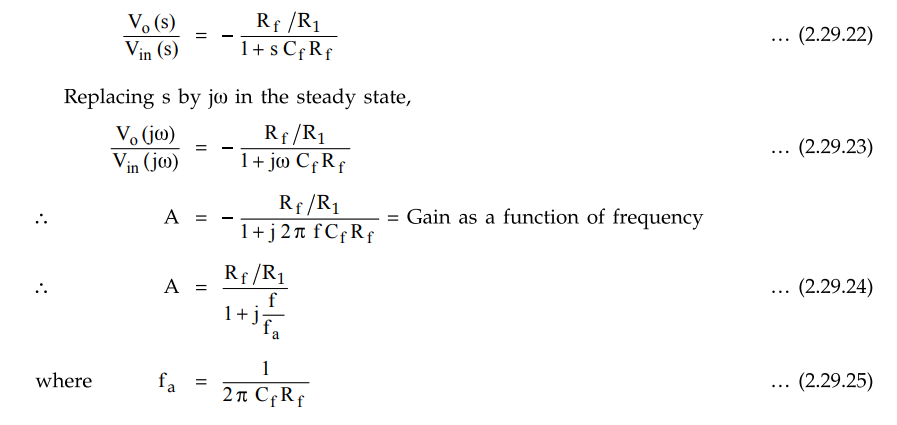
This
is the break frequency or the comer frequency of the practical integrator. Thus
in the frequency response, d.c. gain remains constant for all frequencies less
than fa and from the frequency fa onwards, as frequency
increases, gain reduces at a rate of 20 dB/decade.
The
magnitude of the gain A is,
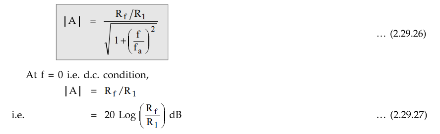
Thus
an infinite d.c. gain of op-amp in case of an ideal integrator, gets limited to
Rf /R1 in the practical integrator.
Similarly
at f = f a we get,
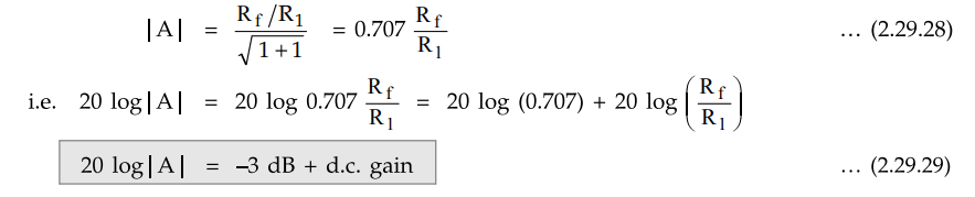
Thus
the magnitude of gain drops by 3 dB at the frequency f = fa which is R 60 the
break frequency. Now for the integration, the frequency response must be
straight line of slope -20 dB/decade, which is possible for the frequencies
greater than fa and less than fb. Thus in between and practical integrator acts
as an integrator. Below fa, integration does not take place. The frequency response
is shown in the Fig. 2.29.9
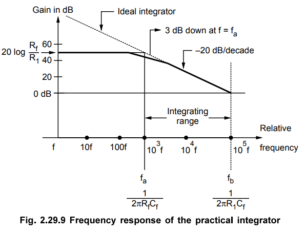
Key Point It can be
seen from the frequency response that the bandwidth of practical integrator is
f a which is much higher than an ideal integrator.
B.W.
of Practical Integrator = fa … (2.29.30)
For
any input bias current or current due to offset voltage, the path of current is
through Rf rather than through the capacitor Cf. Thus the output voltage is
decided by the resistance ratio (Rf/ R1) which is
typically selected as ≥ 10. For (Rf/ R1) of 10, the
frequency fa becomes (fb/10), this ensures the true
integration of the input signal.
For
proper integration, the time period T of the input signal has to be larger than
or equal to RfCf, so
T
≥ RfCf ...
(2.29.31)
where RfCf = 1 / 2π fa
The
practical integrator circuit is also called lossy integrator as it
behaves as integrator only over the upper frequency range.
7. Applications of Practical Integrator
The
integrator circuits are most commonly used in the following applications :
a)
In the analog computers,
b)
In solving the differential equations,
c)
In analog to digital converters.
d)
Various signal wave shaping circuits,
e)
In ramp generators.
8. Why Integrators are Preferred in Analog Computers ?
It
is important to note that the differentiators are avoided in the analog
computer while integrators are widely used in the analog computers. Let us see
the reasons why the integrators are preferred in the analog computers.
i)
The gain of the integrator decreases with increase in the frequency while that
of the differentiator increases with increase in the frequency. Hence it is
very easy to stabilise the integrator with respect to the spurious
oscillations.
ii)
The input impedance of the integrator is constant and not a function of
frequency. While the input impedance of the differentiator decreases as the
frequency increases. So at high frequency the input impedance is very small. If
the input waveform changes rapidly then due to small input impedance, there is
every possibility that the amplifier of the differentiator gets overloaded.
iii)
The differentiator has a tendency to amplify the noise and drifts which may
result in the oscillations. The bandwidth of an integrator is small hence the
integrator is less sensitive to noise voltages.
iv)
The initial voltages present at the output before integration takes place are
called as initial conditions. It is very easy to introduce the initial
conditions in the integrator rather than the differentiator.
v)
Overall the integrator is more stable than the differentiator and less
sensitive to noise and hence chances of oscillations are much less in the
integrator.
Due
to all these reasons the integrators are preferred in the analog computers.
Example
2.29.1 Design a practical integrator circuit with a d.c.
gain of 10, to integrate a square wave of 10 kHz.
Solution
:
The d.c. gain for the practical integrator is
|A|
d.c. = Rf / R1 i.e. 10 = Rf / R1
The
input frequency is f = 10 kHz.
Now
for the proper integration f ≥ 10 fa
where fa is the break frequency of the practical integrator.
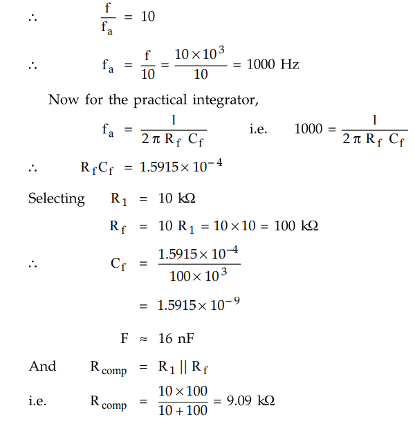
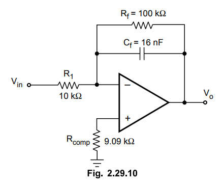
Hence
the practical integrator circuit is as shown in the Fig. 2.29.10.
Example
2.29.2 Plot to scale the output waveform of the circuit
shown in Fig. 2.29.11
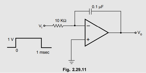
Solution
: The given circuit
is an integrator with R1 = 10 kΩ and C = 0.1 µF.
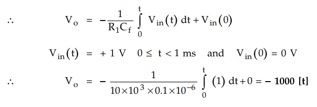
Thus Vo is a straight line of slope - 1000 till 1 ms.
At
t = 1 ms,
Vo
= -1000 × 1 × 10-3 = -1V. This acts as an initial voltage for next
integration.
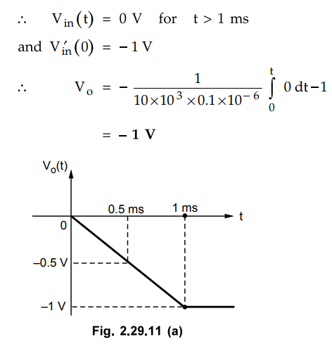
So
after t = 1 ms, the output is constant at - 1 V hence the output waveform is as
shown in the Fig. 2.29.11 (a).
Example
2.29.3 Consider the lossy integrator as shown in Fig.
2.29.12. For the component values R1 = 10 kΩ, Rf - 100 kΩ,
Cf = 1 nF, determine the lower frequency limit of integration and
study the response for the inputs : 1) Step input 2) Square input 3) Sine
input.
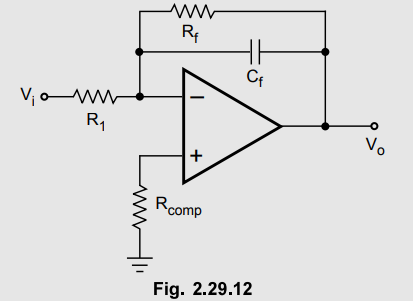
Solution
:
For the practical integrator,
fa
= 1 / 2πRfCf = 1/ 2π × 100 × 103 × 1 × 10-9
= 1.5915 kHz
For
the responses for step, square and sine inputs, refer section 2.29.2.
Review Questions
1. With the circuit diagram explain the operation of an
integrator using op-amp.
Dec.-06,11, May-07,10,12,15, Marks 6
2. Explain why integrators are preferred over differentiators in
analog computers.
May-08, Marks 8
3. Explain and draw the output waveforms of the ideal integrator
circuit when the input is
i. Sine wave ii. Step
input iii. Square wave.
4. Explain the various errors in an ideal integrator circuit.
How these errors are minimized ?
5. Find and Rf in
the loosy integrator so that the peak gain is 40 dB and the gain 3 dB down from
its peak occurs at a frequency of 1.25 kHz. Use capacitance of 0.01 µF
[Ans.: 12.70 kQ, 127 Ql
6. An input d.c. voltage as shown in Fig. 2.29.13 is fed to an
operational amplifier integrator with RC = 1 second. Find the output and
sketch. Opertional amplifier is nulled initially.
May-03, Marks 6
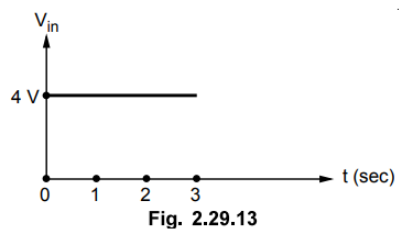
[Ans.: - 4t]
Linear Integrated Circuits: Unit II: Characteristics of Op-amp : Tag: : Working Principle, Waveform, Circuit Diagram, Applications, Solved Example Problems | Operational amplifier - Op-amp Integrator
Related Topics
Related Subjects

Linear Integrated Circuits
EE3402 Lic Operational Amplifiers 4th Semester EEE Dept | 2021 Regulation | 4th Semester EEE Dept 2021 Regulation