Linear Integrated Circuits: Unit II: Characteristics of Op-amp
Op-amp Summer or Adder Circuit
Working Principle, Circuit Diagram, Applications, Solved Example Problems | Operational amplifier
As the input impedance of an op-amp is extremely large, more than one input signal can be applied to the inverting amplifier. Such circuit gives the addition of the applied signals at the output. Hence it is called summer or adder circuit.
Summer or Adder Circuit
As
the input impedance of an op-amp is extremely large, more than one input signal
can be applied to the inverting amplifier. Such circuit gives the addition of
the applied signals at the output. Hence it is called summer or adder circuit.
Depending upon the sign of the output, the summer circuits are classified as
inverting summer and non-inverting summer.
1. Inverting Summer
In
this circuit, all the input signals to be added are applied to the inverting
input terminal of the op-amp. The circuit with two input signals is shown in
the Fig. 2.27.1.
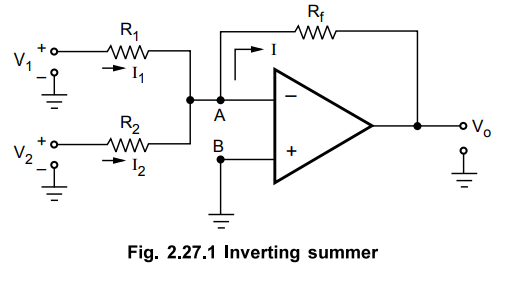
As
point B is grounded, due to virtual ground concept the node A is also at virtual
ground potential.
VA
= 0 .... (2.27.1)
Now
from the input side,
Applying
KCL at node A and as input op-amp current is zero,
I
= I1 + I2 ….. (2.27.4)
From
the output side,
I
= VA – Vo / Rf = - Vo / Rf …. (2.27.5)
Substituting
equations (2.27.5), (2.27.2) and (2.27.3) in equation (2.27.4),
If
the three resistances are equal, R1 = R2 = Rf
Vo
= - ( V1 + V2 )
…. (2.27.7)
By
properly selecting Rf, R1 and R2, we can have
weighted addition of the input signals like aVf + bV2, as indicated by the
equation (2.27.6).
Infact
in such a way, n input voltages can be added.
Key Point Thus the
magnitude of the ouput voltage is the sum of the input voltages and hence
circuit is called summer or adder circuit.
2. Non-inverting Summing Amplifier
The
circuit discussed above is inverting summing amplifier, which can be noticed
from the negative sign in the equation (2.27.6). But a summer that gives
non-inverted sum of the input signals is called non-inverting summing
amplifier. The circuit is shown in the Fig. 2.27.2
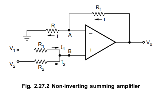
Let
the voltage of node B is VB. NOW the node A is at the same potential
as that of B, due to virtual ground.
VA
= VB …. (2.27.8)
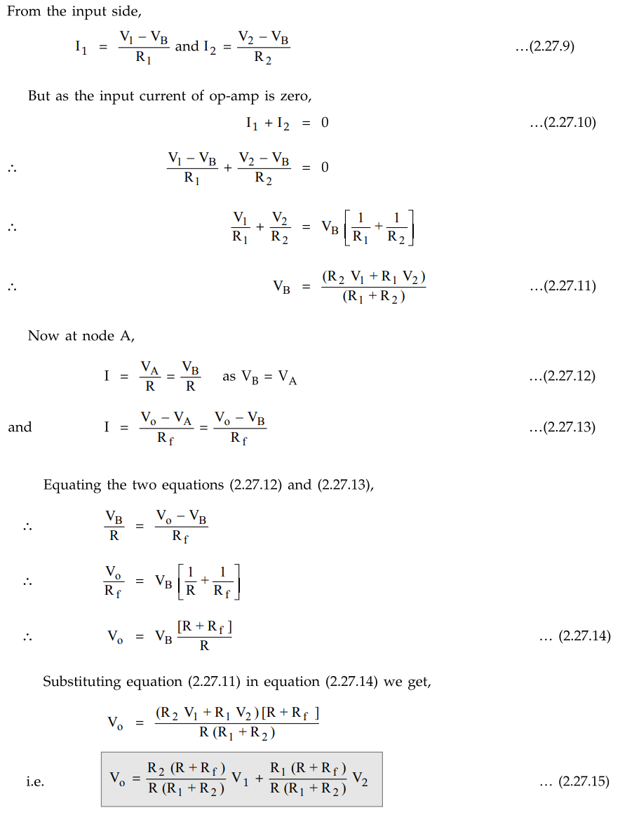
The
equation (2.27.15) shows that the output is weighted sum of the inputs.
If
R1 = R2 = R = Rf, we get
Vo
= V1 + V2 ….
(2.27.16)
Key
Point As there is no phase difference between input
and output, it is called non-inverting summer amplifier.
3. Average Circuit
If
in the inverting summer circuit, the values of resistance are selected as,
R1
= R2 = R
and
Rf = R / 2
Then
from the equation (2.27.6) we get,
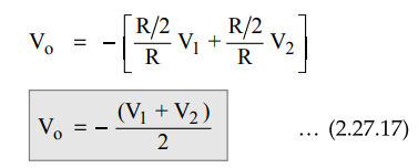
Key Point Thus the magnitude of the output voltage is the average of the two input voltages. So circuit acts like an averager.
Similarly
average of n inputs can be calculated by selecting,
R1
= R2 = R3 = ... = Rn = R and Rf = R
/ n
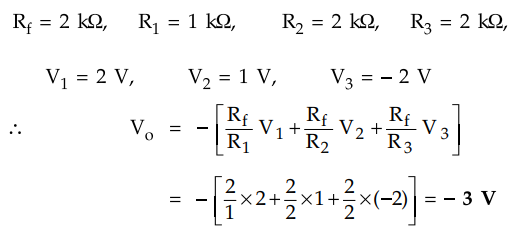
Example
2.27.1 Determine the output voltage for the following
circuit.

Solution
:
This the an inverting summing amplifier.
Example
2.27.2 Determine the output voltage for the circuit
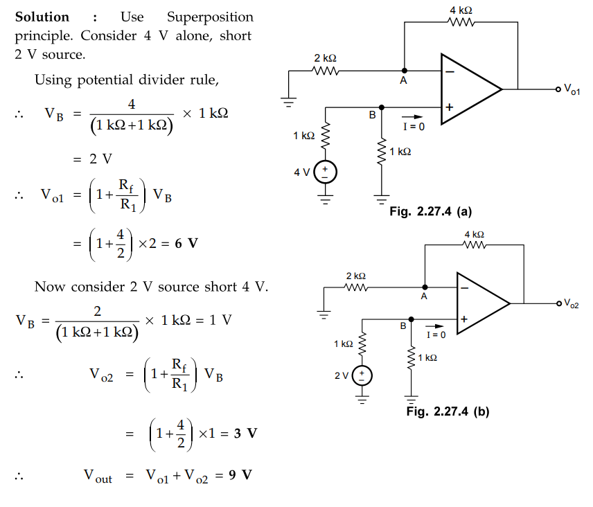
shown in Fig. 2.27.4.
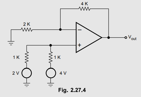
Solution
:
Use Superposition principle. Consider 4 V alone, short 2 V source.
Using
potential divider rule,
Example
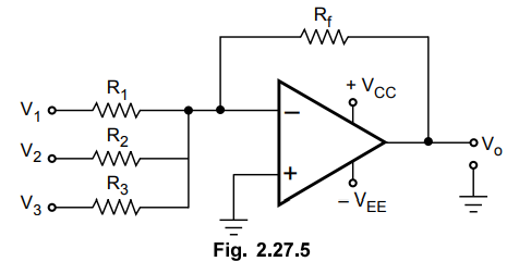
2.27.3 Draw an adder circuit for the given expression Vo
= -(0.1 V1 + V2 +5V3)
Dec.-l0,
Marks 8
Solution
:
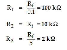
The
adder circuit is shown in the Fig. 2.27.5.
Review Questions
1. Draw and explain the summing amplifier.
2. Explain how the average circuit can be derived from the
summer.
Dec.-09, Marks 2
3. Determine the output voltage for the configuration shown in
the Fig. 2.27.6.
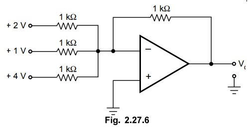
[ Ans.: - 7 V ]
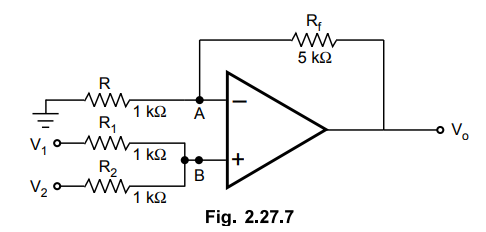
4. Determine the output voltage for the circuit shown in the
Fig. 2.27.7, for V1 = 1 V and V2 = 3 V.
[ Ans.: 12 V ]
5. Calculate the value of Rs in the Fig. 2.27.8 shown, such that
Vo becomes zero.

[Ans.: 6.285 kΩ]
Linear Integrated Circuits: Unit II: Characteristics of Op-amp : Tag: : Working Principle, Circuit Diagram, Applications, Solved Example Problems | Operational amplifier - Op-amp Summer or Adder Circuit
Related Topics
Related Subjects

Linear Integrated Circuits
EE3402 Lic Operational Amplifiers 4th Semester EEE Dept | 2021 Regulation | 4th Semester EEE Dept 2021 Regulation