Linear Integrated Circuits: Unit II: Characteristics of Op-amp
Other Important Op-amp Parameters
Power Supply Rejection Ratio, Slew Rate, Transient Response Rise Time with Solved Example Problems
Two other important op-amp parameters are the slew rate and the Power Supply Rejection Ratio (PSRR). Let us discuss and obtain the expressions for these two parameters.
Other Important Op-amp Parameters
May-2000,03,04,05,06,07,08,10,11,15 Dec.-03,04,05,08,09,10,15, April-05
Two other important op-amp parameters are the slew rate and the Power Supply Rejection Ratio (PSRR). Let us discuss and obtain the expressions for these two parameters.
1. Power Supply Rejection Ratio
The Power Supply Rejection Ratio (PSRR) is defined as the ratio of the change in input offset voltage due to the change in supply voltage producing it, keeping other power supply voltage constant. It is also called Power Supply Sensitivity (PSV).

Now if VEE is constant and due to certain change in VCC, there is change in input offset voltage then PSRR is defined as,
PSRR = ∆ Vios / ∆ VCC ... (2.13.1)
For a fixed VCC, if there is a change in VEE then
PSRR = ∆ Vios / ∆ VEE |constant VCC ... (2.13.2)
As input offset voltage is very small, PSRR is expressed in mV/V or µV/V. The typical value of PSRR for IC 741 op-amp is 30 µV/V.
2. Slew Rate
The slew rate is defined as the maximum rate of change of output voltage with time. The slew rate is specified in V/µsec. Thus

The slew rate is caused due to limited charging rate of the compensating capacitor and current limiting and saturation of the internal stages of an op-amp, when a high frequency, large amplitude signal is applied. The internal capacitor voltage cannot change instantaneously. It is given by dVc/dt = I/C. For large charging rate, the capacitor should be small or charging current should be large.
Hence the slew rate for the op-amp whose maximum internal capacitor charging current is known, can be obtained as
S = Imax/C ... (2.13.4)
For example, for IC 741 the charging current is 15 µA and the internal capacitor is 30 pF, hence its slew rate is
S = 15 × 10-6 / 30 × 10-12 = 0.5 / 10-6 V/sec
i.e. = 0.5 V/µsec
a. Effect of Slew Rate
Consider
a circuit using op-amp having unity gain. Thus output is same as input. If the
input is square wave, output has to be square wave. But this is observed for
certain frequency of input. Due to slew rate of an op-amp, for a particular
input frequency, output gets distorted as shown in the Fig. 2.13.2.

Then
observing such a distorted waveform on CRO the slew rate can be obtained as,
S
= (Δ Vo / Δt ) V/sec
The
typical value of S for IC 741 op-amp is 0.5 × 10⁶ V/sec i.e. 0.5 V/µsec.
Ideally it should be infinite.
Key Point Higher the value
of S, better is the performance of op-amp.
b.
Slew Rate Equation
Consider
unity gain op-amp circuit with purely sinusoidal input. The output must be same
as input.

The
equation (2.13.7) has maximum value when cos ωt = 1.
S
= Vm ω = 2π fVm
S
= 2π fVmV/sec ... (2.13.9)
This
is the required slew rate equation.
For distortion free output, the maximum allowable input frequency fm can be obtained as,
fm = (S / 2πVm) Hz …. (2.13.10)
This is also called full power bandwidth of the op-amp. The Vm is peak of output waveform.
c. Methods of Improving Slew Rate
It is known that the slew rate is given by,
S = Imax / C
For understanding the methods of improving slew rate, consider the op-amp model for the analysis of the slew rate as shown in the Fig. 2.13.3.

The op-amp used is in voltage follower mode, in which the output Vo = Vi. The circuit is similar to that used earlier to derive slew rate equation, only the op-amp is replaced by its model.
When input overdrives the input stage then Imax = ± Iol (sat) which are saturation current levels of the input stage. Under this condition, op-amp is said to be operating under large-signal conditions.
The saturation of the input stage limits the slew rate because under saturation condition, the rate at which capacitor C can charge or discharge, according to the input overdrive is at its maximum.
From the Fig. 2.13.3 we can write,
Iol(sat) = C dVo2 / dt
dVo2 / dt = Iol(sat) / C … (2.13.11)
This rate of change of Vo2 is maximum , due to the saturation effect.
Now the gain of third stage a3 ≈ Vo = Vo2

But maximum rate of change of output voltage is the slew rate.
S = Iol (sat) / C … Slew rate
Analysing the op-amp model used we can write,
Vo2 = drop across C = ZC Iol
The input stage is a transconductance amplifier i.e. voltage input, current output amplifier. For sufficiently small differential input voltage, the relation between input voltage and output current for such an amplifier is,
Output current = gm (differential input)
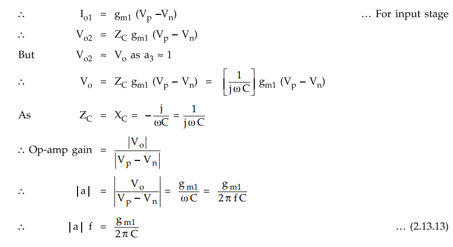
Now the gain-bandwidth product of op-amp is denoted as ft given by the product of gain | a | and bandwidth f as,

The gain bandwidth product is also called unity gain bandwidth of op-amp. Substituting value of C in the slew rate,
S = 2π (Iol(sat) / g ml) ft … (2.13.16)
From this equation, we can get an idea about improvement in slew rate. Hence methods of improving slew rate are,
1. Increasing ft : Higher the value of gain-bandwidth product of op-amp, higher is its slew rate. To increase ft, it can be seen from the equation (2.13.15), the internal capacitor value must be reduced. Hence for uncompensated op-amps, user can use the compensating network in such a way to reduce C and increase ft to improve the slew rate. The frequency compensation schemes like feed-forward compensation, discussed earlier, can be used to achieve high ft and hence higher slew rate.
2. Increasing Io1(sat) : This method is difficult because Iol(sat) for the op-amp can not be controlled externally by the user. But to increase Iol without affecting the value of gml and ft is to provide alternative path to the rapid charging and discharging of C, when large signal condition exists. This is possible by using additional input transistor pair which can be designed such that it will go into conduction region when sufficiently large amplitude input signal is applied. This can increase Iol(sat) to improve the slew rate.
But such adjustments are possible only in programmable op-amps where operating point of the device can be set by the user with external current Iset. The separate pin is provided for such op-amps to implement such current setting. Examples of such programmable op-amps are µA776 by Fairchild, LM346 by National Semiconductor, TL066 by Texas Instruments etc.
3. Reducing gm1 : The gain of transistorised differential input stage can be reduced by using suitable resistances in series with the emitters of the differential input transistors. This technique is called emitter degeneration. Reducing input stage transconductance by this method, slew rate can be improved.
Another method of reducing transconductance of the input stage is to use FET differential input pair instead of BJT differential input pair. The gm values for the FETs are less than those for the BJTs. In addition to reducing gm and improving slew rate, the added advantages of using FETs are very low input bias currents and very low input offset currents.
Thus by using proper frequency compensation and other compensating networks and referring to the data sheets, higher slew rate op-amps can be selected for the high speed applications.
Example 2.13.1 An op-amp operates as a unity gain buffer with 3 V (peak to peak) square wave input. If op-amp is ideal with slew rate 0.5 V/µ sec find the maximum frequency of operation.
Solution : Given circuit is unity gain.
Peak to peak = 3 V of square wave

3. Transient Response Rise Time
When the output of the op-amp is suddenly changing like pulse type, then the rise time of the response depends on the cut-off frequency fH of the op-amp. Such a rise time is called cut-off frequency limited rise time or transient response rise time. It is inversely proportional to the cut-off frequency and given by,
tr = 0.35 / fH
where tr = Rise time and fH = Cut-off frequency.
Example 2.13.2 The open loop gain of a certain op-amp falls to 0 dB at a frequency of 10 MHz. Find the transient response rise time, if it is used as unity gain amplifier. April-05, Marks 4
Solution : For unity gain amplifier, UGB = fH = 10 MHz given.
tr = 0.35 / fH = 0.35 / 10 × 106 = 35 nsec ... Rise time
Example 2.13.3 For an op-amp having a slew rate of 3 V / psec. What is the maximum closed loop voltage gain that can be used when the input signal varies fcy 0.4 V in 12 µsec ?
Solution : Let A be the closed loop gain.
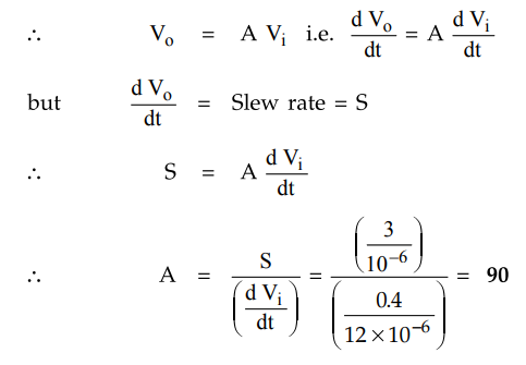
Any closed loop gain of magnitude greater than 90 would drive the output at a rate greater than the slew rate allows, so the maximum closed loop gain is 90.
Example 2.13.4 An op-amp has 7 kHz sine wave input signal. Find the largest amplitude that the output of the amplifier can have without distortion with ICQ of 8 µA and CC of 27 pF.
Solution : The slew rate is,

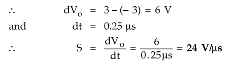
Example 2.13.5 In response to a square wave input, the output of an op-amp changed from -3 V to +3 V over a time interval of 0.25 µs. Determine the slew rate of the op-amp. Dec.-04, May-06, Marks 6
Solution : Change in output voltage = - 3 V to + 3 V
Review Questions
1. Define slew rate. Explain the causes of slew rate. Derive slew rate equation for op-amp voltage follower.
2. An op-amp 741 with a slew rate of 0.5 Vfosec is used in a noninverting amplifier with gain of 2. Determine the highest frequency that may be processed that will produce output of 20 V peak to peak without exceeding slew rate.
[ Ans.: 7.95 kHz ]
3. The input signal Vi to an op-amp is 0.04 sin 1.13 × 10⁵ t is to be amplified to the maximum extent. How much maximum gain can be had by using op-amp with slew rate of 0.4 V/µsec ?
[ Ans.: 88.5 ]
4. What is slew rate ? Explain the methods used to improve the slew rate. May-07, 15, Marks 8
Linear Integrated Circuits: Unit II: Characteristics of Op-amp : Tag: : Power Supply Rejection Ratio, Slew Rate, Transient Response Rise Time with Solved Example Problems - Other Important Op-amp Parameters
Related Topics
Related Subjects

Linear Integrated Circuits
EE3402 Lic Operational Amplifiers 4th Semester EEE Dept | 2021 Regulation | 4th Semester EEE Dept 2021 Regulation