Linear Integrated Circuits: Unit II: Characteristics of Op-amp
Output Offset Voltage(Voos) in Op-amp
Thus the d.c. voltage present at the output terminals when both the input terminals are grounded is called output offset voltage denoted as Voos.
Output Offset Voltage(Voos)
The
effect of input bias current, input offset current and input offset voltage is
to add the error to the expected d.c. output voltage. These parameters produce
the output voltage when both the input terminals are grounded.
Thus
the d.c. voltage present at the output terminals when both the input terminals
are grounded is called output offset voltage denoted as Voos.
The
output voltage caused by input offset voltage Vios can be either positive or
negative with respect to ground. Similarly, the output voltage due to the input
bias current Ib2 can be also positive or negative with respect to ground. If
these output voltages are of different polarity then the total output offset
voltage is very small. But if these voltages are of same polarity then output
offset voltage is large. Thus the output offset voltage is given by,
Voos
= Vo due to Vios + Vo due to Ib
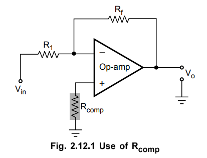
To
compensate the output offset voltage due to the input bias current a compensating
resistance is used as shown in the Fig. 2.12.1. It is denoted as Rcomp.
This is called offset minimizing resistor.
While
the effect of offset voltage is nullified using voltage compensating network.
For
many op-amps, the offset compensation pins are provided to nullify the offset
voltage. The manufacturer's specifications must be referred to use these
compensation pins. For example, in case of IC 741 op-amp, the pins 1 and 5 are
provided as compensation pins. The manufacturer recommends that a 10 kΩ potentiometer
must be connected between the pins 1 and 5.
A
wiper must be connected to the negative supply pin which is pin number 4. By
adjusting this potentiometer wiper, the output can be nullified.
The
arrangement for IC 741 op-amp is shown in the Fig. 2.12.2.

If
the op-amp does not have the offset compensation pins, then the separate
external compensating network is required to be designed.
Review Question
1. Define output offset voltage. Explain a method to nullify
offset voltage.
Dec.-05, May-11, Marks 6
Linear Integrated Circuits: Unit II: Characteristics of Op-amp : Tag: : - Output Offset Voltage(Voos) in Op-amp
Related Topics
Related Subjects

Linear Integrated Circuits
EE3402 Lic Operational Amplifiers 4th Semester EEE Dept | 2021 Regulation | 4th Semester EEE Dept 2021 Regulation