Microprocessors and Microcontrollers: Unit III: (a) 8051 Microcontroller
Pin Description of 8051
Review Questions : 1. Draw the pin diagram of 8051 microcontroller and explain its port structure. 2. List the alternative functions assigned to Port 3 pins of 8051 microcontroller. 3. Explain the pinouts of 8051 microcontroller. Internal and External Memories
Pin Description of 8051
The
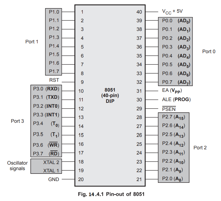
8051 is packaged in a 40-pin DIP. The Fig. 14.4.1 shows the pin diagram of
8051. It is important to note that many pins of 8051 are used for more than one
function. The alternative functions of pins are shown in bold letters.
The
8051 has 32 I/O pins configured as four eight-bit parallel ports (P0, Pl, P2
and P3). All four ports are bidirectional i.e. each pin will be configured as
input or output (or both). All port-pins are multiplexed except the pins of
port 1. Each port consists of a latch, an output driver and an input buffer.
Port
0 (Pins 32 - 39) : Port 0 pins can be used as I/O pins. The
output drives and input buffers of port 0 are used to access external memory.
Port 0 outputs the low order byte of the external memory address, time
multiplexed with the data being written or read. Thus, port 0 can be used as a
multiplexed address/data bus.
Port
1 (Pins 1 - 8) : Port 1 pins can be used only as I/O
pins.
Port
2 (Pins 21 - 28) : The output drives of port 2 are used to
access external memory. Port 2 outputs the high order byte of the external
memory address when the address is 16 bits wide. Otherwise, port 2 is used as
an I/O port.
Port
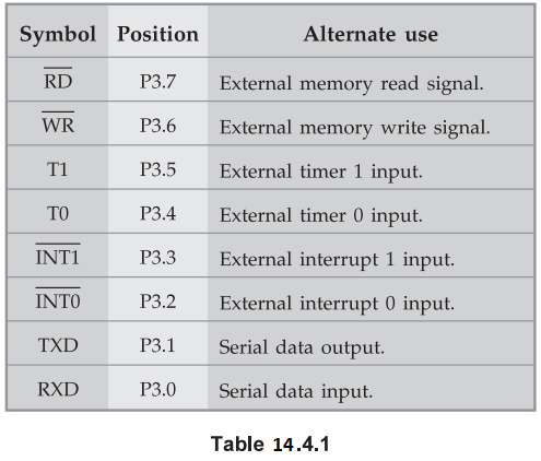
3 (Pins 10 - 17) : All port pins of port 3 are
multifunctional. Therefore, each pin of port 3 can be programmed to use as I/O
or as one of the alternate function. They have special functions as shown below
including two external interrupts, two counter inputs, two special data lines
and two timing control strobes.
Power-supply
Pins VCC (Pin 40) and VSS (Pin 20) :
8051 operates on d.c. power supply of +5 V with respect to ground. The +5 V is
to be connected to pin VCC and ground to pin VSS with
rated power supply current of 125 mA.
Oscillator
Pins XTAL2 (Pin 18) and XTAL1 (Pin 19) : For generating an
internal clock signal, the external oscillator is connected at these two pins.
ALE
(Address Latch Enable, Pin 30) : AD0 to AD7
lines are multiplexed. To demultiplex these lines and for obtaining lower half
of an address, an external latch and ALE signal of 8051 is used.
RST
(Reset, Pin 9) : This pin is used to reset 8051. For
proper reset operation, reset signal must be held high at least for two machine
cycles, while oscillator is running.
 (Program Store Enable, Pin 29) : It is the active low
output control signal used to activate the enable signal of the external
ROM/EPROM. It is activated every six oscillator periods while reading the
external memory. Thus, this signal acts as the read strobe to external program
memory.
(Program Store Enable, Pin 29) : It is the active low
output control signal used to activate the enable signal of the external
ROM/EPROM. It is activated every six oscillator periods while reading the
external memory. Thus, this signal acts as the read strobe to external program
memory.
![]() (External Access, Pin 31) : When the
(External Access, Pin 31) : When the ![]() pin is high
(connected to VCC), program fetches to addresses 0000H through 0FFFH
are directed to the internal ROM and program fetches to addresses 1000H through
FFFFH are directed to external ROM/EPROM. When
pin is high
(connected to VCC), program fetches to addresses 0000H through 0FFFH
are directed to the internal ROM and program fetches to addresses 1000H through
FFFFH are directed to external ROM/EPROM. When ![]() is low (grounded),
all addresses (0000H to FFFFH) fetched by program are directed to the external
ROM/EPROM.
is low (grounded),
all addresses (0000H to FFFFH) fetched by program are directed to the external
ROM/EPROM.
Review Questions
1. Draw the pin
diagram of 8051 microcontroller and explain its port structure. AU : Dec.-11, Marks 8
2. List the
alternative functions assigned to Port 3 pins of 8051 microcontroller. AU : May-11, Marks 2
3. Explain the pinouts of 8051 microcontroller. Internal and External Memories AU : Dec.-10, 11, 12, 16, 17, 19, May-11
Microprocessors and Microcontrollers: Unit III: (a) 8051 Microcontroller : Tag: : - Pin Description of 8051