Microprocessors and Microcontrollers: Unit I: (a) 8085 Processor
Pin diagram of 8085
Power Supply and Frequency Signals - Data Bus and Address Bus - Control and Status Signals - Interrupt Signals - Serial I/O signals - DMA Signal - Reset Signals
Questions : 1. Write about the pin configuration of 8085 processor and explain them in detail. 2. Draw the signal configuration of 8085 and explain the purpose of each signals. 3. What is the use of ALE signal ? 4. What is the use of CLKOUT and RESET OUT signals of 8085 processor ? 5. Draw the pin diagram of 8085 microprocessor and list the classification of signals.
Pin diagram of 8085
AU
: May - 09, 12, 14, 17, 18, Dec.-12, 14
Fig.
1.3.1 (a) and (b) show 8085 pin configuration and functional pin diagram of
8085 respectively. The signals of 8085 can be classified into seven groups
according to their functions.
a)
Power supply and frequency signals.
b)
Data bus and address bus
c)
Control bus
d)
Interrupt signals
e)
Serial I/O signals
f)
DMA signals
g)
Reset signals
1. Power Supply and Frequency Signals
i)
VCC : It requires a single +5 V power supply.
ii)
VSS : Ground reference.
iii)
X1 and X2 : A tuned circuit like
LC, RC or crystal is connected at these two pins. The internal clock generator
divides oscillator frequency by 2, therefore, to operate a system at 3 MHz, the
crystal of tuned circuit must have a frequency of 6 MHz.
iv)
CLK OUT : This signal is used as a system clock for other
devices. Its frequency is half the oscillator frequency.

2. Data Bus and Address Bus
A)
AD0 to AD7
:
The 8-bit data bus (D0 - D7) is multiplexed with the
lower half (A0 - A7) of the 16-bit address bus. During
first part of the machine cycle (T1), lower 8 bits of memory address or I/O
address appear on the bus. During remaining part of the machine cycle (T2
and T3) these lines are used as a bi-directional data bus.
B)
A8 to A15 : The upper half of the
16-bit address appears on the address lines A8 to A15.
These lines are exclusively used for the most significant 8 bits of the 16-bit
address lines.
3. Control and Status Signals
A)
ALE (Address Latch Enable) : We know that AD0
to AD7 lines are multiplexed and the lower half of address (A0
- A7) is available only during T1 of the machine cycle.
This lower half of address is also necessary during T2 and T3
of machine cycle to access specific location in memory or I/O port. This means
that the lower half of an address must be latched in T1 of the
machine cycle, so that it is available throughout the machine cycle. The
latching of lower half of an address bus is done by using external latch and
ALE signal from 8085.
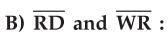 A low on
 ![]() indicates that the data must be read from the selected
memory location or I/O port via data bus. A low on
indicates that the data must be read from the selected
memory location or I/O port via data bus. A low on ![]() p indicates that
the data must be written into the selected memory location or 1/O port via data
bus.
p indicates that
the data must be written into the selected memory location or 1/O port via data
bus.
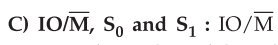 indicates whether I/O operation or
memory operation is being carried out. S1 and S0 indicate
the type of machine cycle in progress.
indicates whether I/O operation or
memory operation is being carried out. S1 and S0 indicate
the type of machine cycle in progress.
D)
READY : It is used by the microprocessor to sense whether a
peripheral is ready or not for data transfer. If not, the processor waits. It
is thus used to synchronize slower peripherals to the microprocessor.
4. Interrupt Signals
The
8085 has five hardware interrupt signals : RST 5.5, RST 6.5, RST 7.5, TRAP and
INTR. The microprocessor recognizes interrupt requests on these lines at the
end of the current instruction execution.
The  (Interrupt Acknowledge) signal is used to indicate that the processor
has acknowledged an INTR interrupt.
(Interrupt Acknowledge) signal is used to indicate that the processor
has acknowledged an INTR interrupt.
5. Serial I/O signals
A)
SID (Serial I/P Data) : This input signal is used to
accept serial data bit by bit from the external device.
B)
SOD (Serial O/P Data) : This is an output signal which
enables the transmission of serial data bit by bit to the external device.
6. DMA Signal
A) HOLD : This signal indicates that
another master is requesting for the use of address bus, data bus and control
bus.
B)
HLDA : This active high signal is used to acknowledge HOLD
request.
7. Reset Signals
A)  : A low on this pin
1)
Sets the program counter to zero (0000H) and clears the INTE flag.
2)
Resets the interrupt enable and HLDA flip-flops.
3)
Tri-states the data bus, address bus and control bus. (Note : Only during RESET
is active).
4)
Affects the contents of processor's internal registers randomly.
B)
RESET OUT : This active high signal indicates that
processor is being reset. This signal is synchronized to the processor clock
and it can be used to reset other devices connected in the system.
Review Questions
1. Write about the pin
configuration of 8085 processor and explain them in detail.
AU : June-09, May-17,
Marks 16
2. Draw the signal
configuration of 8085 and explain the purpose of each signals.
AU : May-14, Marks 16
3. Draw the pin
diagram of 8085 microprocessor.
AU : June-12, Marks 4
4. Explain different
control signals used by 8085.
AU : Dec.-14, Marks 8
5. What is the use of
ALE signal ?
6. What is the use of
CLKOUT and RESET OUT signals of 8085 processor ?
7. Describe the
function of following pins in 8085.

8. Explain the signals
used in DMA operation in 8085.
9. Draw the pin
diagram of 8085 microprocessor.
AU : May-12, Marks 4
10. Draw the pin
diagram of 8085 microprocessor and list the classification of signals.
AU : Dec.-12, Marks 8
11. Draw and explain
the building blocks and its signal of 8085 processor.
AU : May-18, Marks 13
Microprocessors and Microcontrollers: Unit I: (a) 8085 Processor : Tag: : Power Supply and Frequency Signals - Data Bus and Address Bus - Control and Status Signals - Interrupt Signals - Serial I/O signals - DMA Signal - Reset Signals - Pin diagram of 8085
Related Topics
Related Subjects
Microprocessor and Microcontroller
EE3404 MCU 4th Semester EEE Dept | 2021 Regulation | 4th Semester EEE Dept 2021 Regulation