Digital Logic Circuits: Unit IV: (c) Introduction to Programmable Logic Devices
PLA (Programmable Logic Array)
Concept, Architecture, Block diagram, Working principle, Applications, Example Problems
• The combinational circuit do not use all the minterms every time. Occasionally, they have don't care conditions. Don't care condition when implemented with a PROM becomes an address input that will never occur.
PLA (Programmable Logic Array)
Dec.-05,
06, 08, 12, 16, 17, May-08, 09, 10, 11, 17
•
The combinational circuit do not use all the minterms every time. Occasionally,
they have don't care conditions. Don't care condition when implemented with a PROM
becomes an address input that will never occur. The result is that not all the
bit patterns available in the PROM are used, which may be considered a waste of
available equipment.
•
For cases where the number of don't care conditions is excessive, it is more
economical to use a second type of LSI component called a Programmable Logic
Array (PLA). A PLA is similar to a PROM in concept; however it does not provide
full decoding of the variables and does not generates all the minterms as in
the PROM. The PLA replaces decoder by group of AND gates, each of which can be
programmed to generate a product term of the input variables. In PLA, both AND
and OR gates have fuses at the inputs, therefore in PLA both AND and OR gates
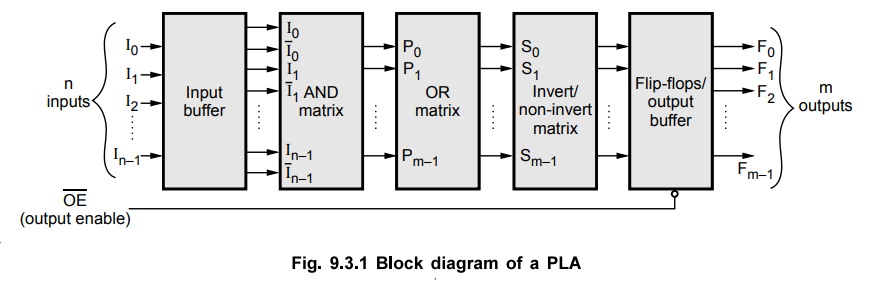
are programmable. Fig. 6.6.17 shows the block diagram of PLA. It consists of
n-inputs, output buffer with m outputs, m product terms, m sum terms, input and
output buffers. The product terms constitute a group of m AND gates and the sum
terms constitute a group of m OR gates, called OR matrix. Fuses are inserted
between all n-inputs and their complement values to each of the AND gates.
Fuses are also provided between the outputs of the AND gates and the inputs of
the OR gates. The third set of fuses in the output inverters allows the output function
to be generated either in the AND-OR form or in the AND-OR-INVERT form. When
inverter is bypassed by link we get AND-OR implementation. To get
AND-OR-INVERTER implementation inverter link has to be disconnected.
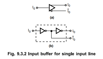
1. Input Buffer
•
Input buffers are provided in the PLA to limit loading of the sources that
drive the inputs. They also provide inverted and non-inverted form of inputs at
its output. The Fig. 9.3.2 shows two ways of representing input buffer for
single input.
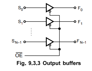
2. Output Buffer
The
driving capacity of PLA is increased by providing buffers at the output. They
are usually 1 IL compatible. The Fig. 9.3.3 shows the tri-state, 1 IL
compatible output buffer. The output buffer may provide totem-pole, open collector
or tri-state output.
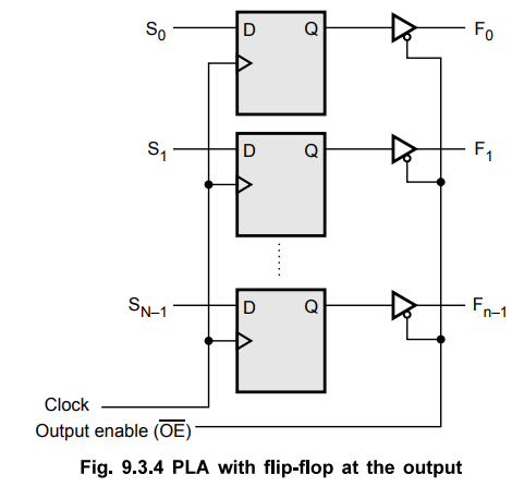
3. Output through Flip-Flops
For
the implementation of sequential circuits we need memory elements, flip-flops
and combinational circuitry for deriving the flip-flop inputs. To satisfy both
the needs some PLAs are provided with flip-flop at each output, as shown in the
Fig. 9.3.4.
4. Implementation of Combination Circuit using PLA
•
Like ROM, PLA can be mask-programmable or field-programmable. With a
mask-programmable PLA, the user must submit a PLA program table to the
manufacturer. This table is used by the vendor to produce a user-made PLA that
has the required internal paths between inputs and outputs. A second type of
PLA available is called a field-programmable logic array or FPLA. The FPLA can
be programmed by the user by means of certain recommended procedures. FPLAs can be programmed with
commercially available programmer units.
•
As mentioned earlier, user has to submit PLA program table to the manufacturers
to get the user-made PLA. Let us study how to determine PLA program table with
the help of example.
Examples
for Understanding
Ex.
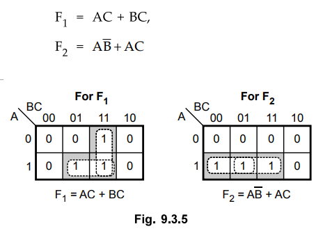
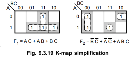
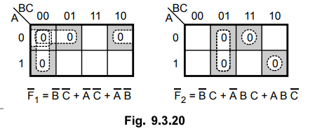
9.3.1 A combinational circuit is defined by the functions :
F1
= ∑ m (3,5,7), F2 = ∑ m (4,5,7)
Implement
the circuit with a PLA having 3 inputs, 3 product terms and two outputs.
Solution
:
Step
1 :
Simplify the given Boolean functions
The
Boolean functions are simplified, as shown in the Fig. 9.3.5. The simplified
functions in sum of products are obtained from the maps are :
Step
2 : Write
PLA program table

Therefore,
there are three distinct product terms : AC, BC and AB, and two sum terms. The
PLA program table shown in Table 9.3.1 consists of three columns specifying
product terms, inputs and outputs. The first column gives the lists of product
terms numerically. The second column specifies the required paths between
inputs and AND gates. The third column specifies the required paths between the
AND gates and the OR gates. Under each output variable, we write a T (for true)
if the output inverter is to be bypassed, and C (for complement) if the
function is to be complemented with the output inverter. The product terms
listed on the left of first column are not the part of PLA program table they
are included for reference only.
Step
3 : Implementation

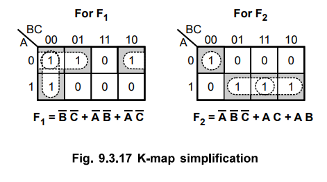
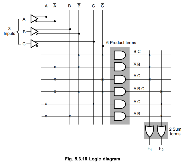
Ex.
9.3.2 Draw a PLA circuit to implement the logic functions
Sol.
:
Step
1 :
Simplify the Boolean functions
Note
:
The second Boolean function is in simplified form.
Step
2 :
Implementation

Ex.
9.3.3 Implement the following multiboolean function using 3 × 4 × 2 PLA PLD.
f1
(a2, a1, a0 ) = ∑ m (0, 1, 3, 5) and
f2
(a2, a1, a0 ) = ∑ m (3, 5, 7)
Sol.
:
Step
1 : Simplify
the Boolean functions.
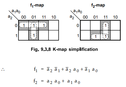
To
implement functions fj. and f2 we require 3 x 5 x 2 PLA and we have to
implement them using 3x4x2 PLA. Therefore, we have to examine product terms by
grouping Os instead of 1. That is product terms for complement of a function.
Step
2 :
Implementation
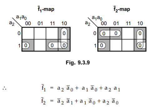
Looking
at function outputs we can realize that product terms 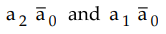 are common in
both functions. Therefore, we need only 4 product terms and functions can be
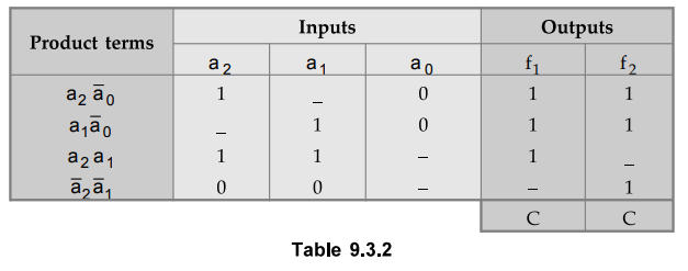
implemented using a 3 × 4 × 2 PLA as shown in Table 9.3.2 and Fig. 9.3.10.
are common in
both functions. Therefore, we need only 4 product terms and functions can be
implemented using a 3 × 4 × 2 PLA as shown in Table 9.3.2 and Fig. 9.3.10.
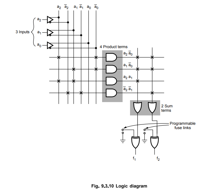
PLA
As shown in the Fig. 9.3.10 exclusive-OR gate is programmed to invert the function to get the desired function outputs.
Ex.
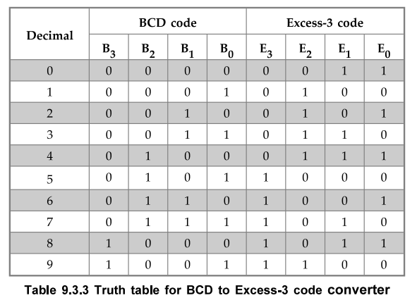
9.3.4 Design a BCD to Excess-3 code converter and implement using suitable PLA.
Sol.
:
Step
1 :
Derive the truth table of BCD to Excess-3 converter
Step
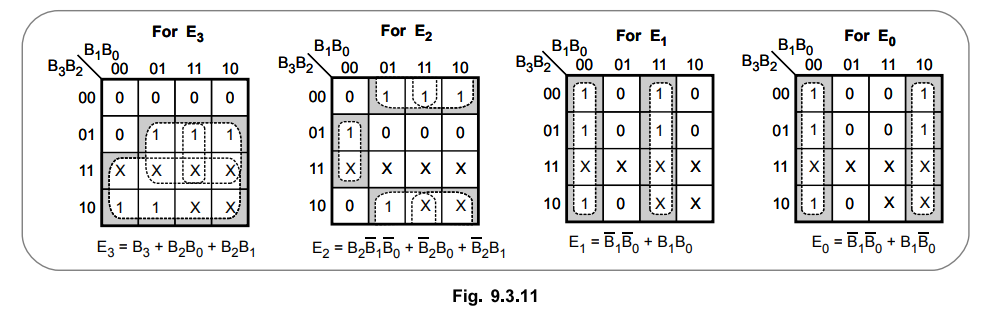
2 :
Simplify the Boolean functions for Excess-3 code
Step
3 : Write
PLA program table

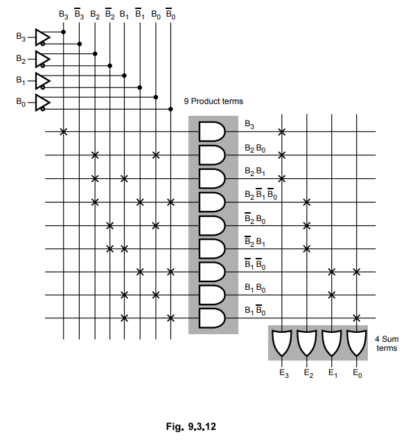
Step
4 : Implementation
Examples
with Solutions
Ex.
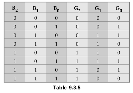
9.3.5 Design and implement 3-bit binary to gray code converter using PLA.
Sol.
:
Step
1 :
Derive the truth table for 3-bit binary to gray code converter
Step
2 :
Simplify the Boolean functions for gray code

Step
3 :
Implementation

Ex.
9.3.6 Design a combinational circuit using PLA. The circuit accepts 3-bit
number and generates an output binary number equal to square of input number.
Sol
. :
Step
1 :
Derive the truth table
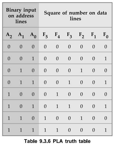
Step
2 : Simplify
Boolean functions of square output
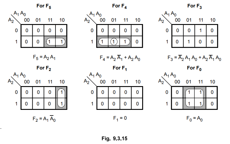
Step
3 : Implementation

Ex.
9.3.7 Implement the following two Boolean functions with a PLA.
F1
(A, B, C) = ∑ (0, 1, 2, 4)
F2
(A, B, C) = ∑ (0, 5, 6, 7)
Sol
. :
Step
1 :
Simplify the Boolean function
Step
2 :
Implementation
Ex.
9.3.8 A combinational circuit is defined by functions.
F1
(A, B, C) = ∑ (3, 5, 6, 7)
F1
(A, B, C) = ∑ (0, 2, 4, 7).
Implement
the circuit with a PLA having three inputs, four product terms and two outputs.
AU
: Dec.-05, Marks 6
Sol
. :
Step
1 :
Simplify the Boolean functions
Here,
we have 6 product terms so we check for complement functions.
If
we take  outputs of two functions, we need only four product
terms since product terms
outputs of two functions, we need only four product
terms since product terms 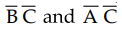 are common between them.
Step
2 : Implementation
Ex.
9.3.9 Design a PLA structure using AND and OR logic for the following functions.
F1
= ∑m (0, 1, 2,
3, 4, 7, 8, 11, 12, 15)
F2
= ∑m (2, 3, 6,
7, 8, 9, 12, 13)
F3
= ∑m (1, 3, 7,
8, 11, 12, 15)
F4
= ∑ m (0, 1,
4, 8, 11, 12, 15)
Sol.
:
Step
1 :
Simplify Boolean functions
AU
: Dec.-16, Marks 10

Step
: 2
Implementation

Examples
for Practice
Ex.
9.3.10 Implement the following Boolean functions with a PLA
F1
(A, B, C) = ∑ (0, 1, 2, 4)
F2
(A, B, C) = ∑ (0, 5, 6, 7)
F3
(A, B, C) = ∑ (0, 3, 5, 7).
Ex.
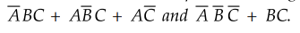
9.3.11 A combinational circuit is defined as the functions
F1
= AB’C’ + AB’C + ABC
F2
= A’BC + AB’C + ABC
Implement
the digital circuit with a PLA having 3 inputs, 3 product terms, and 2 outputs.
Ex.
9.3.12 Draw a PLA circuit to implement the functions
F1
= A'B + AC + ABC ; F2 = (AC + AB + BC).
Ex.
9.3.13 Design and implement a 4-bit
binary to Gray code converter using a PLA.
Ex.
9.3.14 Design an AND-OR-PLA that
implements the functions
f(x,
y, z) = ∑m (0, 2, 4, 6)
g(x,
y, z) = ∑m (1, 3, 5, 7).
Review Questions
1. Discuss the concept, working and applications of PLA.
2. What is a PLA ?
3. How does the architecture of a PLA different from a PROM ?
AU : May-09, Marks 2
Digital Logic Circuits: Unit IV: (c) Introduction to Programmable Logic Devices : Tag: : Concept, Architecture, Block diagram, Working principle, Applications, Example Problems - PLA (Programmable Logic Array)
Related Topics
Related Subjects

Digital Logic Circuits
EE3302 3rd Semester EEE Dept | 2021 Regulation | 3rd Semester EEE Dept 2021 Regulation