Linear Integrated Circuits: Unit III: Applications of Op-amp
Precision Rectifiers using Op-amp
Working Principle, Pulse, Circuit Diagram | Operational amplifier
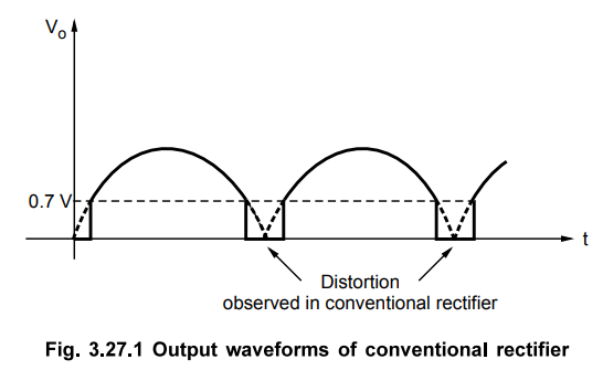
Recall from basic circuit principles that a rectifier circuits can be implemented with a diode/diodes (half wave rectifier or full wave rectifier). The major limitations of these circuits is that they cannot rectify voltages below VD(ON) = 0.7 V, the cut-in voltage of the diode.
Precision Rectifiers
May-04,11 Dec.-05, 06, 07,09
Recall from basic circuit principles that a
rectifier circuits can be implemented with a diode/diodes (half wave rectifier
or full wave rectifier). The major limitations of these circuits is that they
cannot rectify voltages below VD(ON) = 0.7 V, the cut-in voltage of
the diode. In these circuits V; has to rise to a threshold of the order of
VD(ON) before any appreciable change can be seen at the output.
Therefore, above this threshold we have Vo
= Vi - VD(ON) threshold Vi= 0.7 V and below i.e. threshold Vo= 0 i.e.
Vo = Vi - VD(ON) for Vi ≥ VD(ON) … (3.27.1.(a))
Vo = 0 V for Vi
≤ VD(ON) … (3.27.1.(b))
Due to this, output of the conventional rectifier is distorted, as shown in the Fig. 3.27.1.
To achieve precision rectification we need a
circuit that keeps Vo equal to Vi for Vi > 0V. This can be achieved by using
op-amp along with the diodes and these circuits are called precision
rectifiers. These are used to precisely rectify voltages having amplitudes less
than 0.7 V. Hence these circuits are called small signal precision rectifiers.
1. Precision Half Wave Rectifiers
The precision half wave rectifiers are
classified as,
1. Positive half wave rectifier 2. Negative
half wave rectifier
a.
Positive Precision Half Wave Rectifier
The
Fig. 3.27.2 shows the positive small signal precision half wave rectifier.
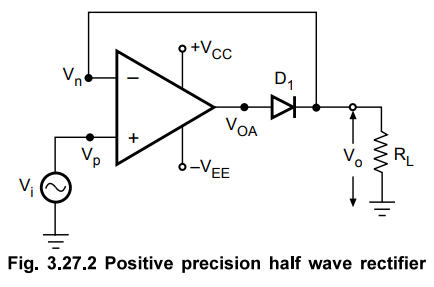
The
diode D1 is used in the feedback loop of the circuit. The analysis
can be done for Vi > 0 V and Vi < 0 V.
Case
1 : Vi > 0 V
Consider
that input voltage is positive going. Due to high open loop gain of op-amp it
produces high voltage VOA. This provides enough drive to the diode D1 to make
it forward biased. So it acts as a ideal diode and in forward biased condition
behaves as a switch as shown in the Fig. 3.27.3.
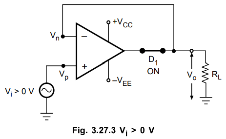
The
cut-in voltage of diode of 0.7 V gets divided by AOL which is very
high. Hence immediately when Vi starts increasing, D1
becomes ON.
Then
circuit works as a voltage follower. From virtual ground Vn = Vp
= Vi and Vo = Vn due to the feedback path.
Hence entire positive half cycle is available across the load.
Case
2 : Vi < 0 V
When
Vi goes negative, immediately VOA produced attains - Vsat value
making diode Di reverse biased. Thus diode D1 acts as an open circuit as shown
in the Fig. 3.27.4.
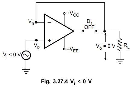
Due
to OFF diode D1, feedback path gets opened and no current can flow
through RL. The voltage Vo is 0 V and negative half cycle of Vi
gets clipped from the output.
The
input-output waveforms are shown in the Fig. 3.27.5.
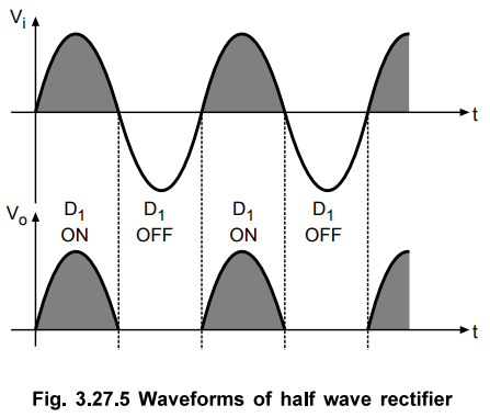
Thus
compared to conventional rectifiers, precision rectifiers can rectify very
small voltages of the order of few millivolts.
Key
Point For positive input cycle, the positive output
cycle exists at the output hence the circuit is also called non-inverting half
wave precision rectifier.
b.
Negative Precision Half Wave Rectifier
By
changing the direction of D1 in positive half wave rectifier
circuit, the negative half wave rectifier can be obtained. It is shown in the
Fig. 3.27.6.
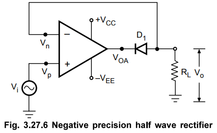
When
Vi > 0 V i.e. positive
going, immediately VOA is very high due to high open loop gain. This reverse
biases the diode, making it open. Thus Vo = 0 V as no current can
pass through RL.
When
Vi < 0 V i.e. negative going, instantaneously VOA is
highly negative which forward biases the diode Dx making it ON. It acts as
short circuit and the circuit acts as a voltage follower. Hence the output
voltage is same as input voltage. Thus the entire negative half cycle is
available across the load. Hence the circuit is called negative half wave
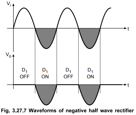
rectifier. The waveforms are as shown in the Fig. 3.27.7.
Another
type of negative half wave rectifier which acts as an inverting precision half
wave rectifier is shown in the Fig. 3.27.8.
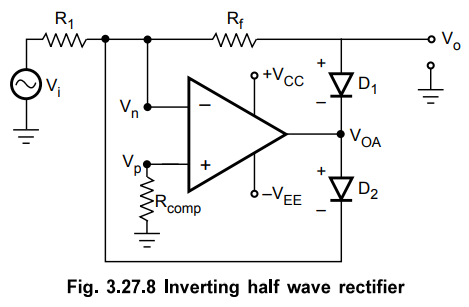
The
basic op-amp circuit is used in inverting mode and the input is applied to
inverting input terminal. When Vi > 0 V i.e. positive going, due to high open
loop gain VOA is highly negative.
This
forward biases the diode D1 and reverse biases D2 and
circuit becomes as shown in the Fig. 3.27.9.
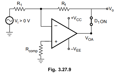
Thus
it acts as an inverting amplifier as feedback path gets established through ON
diode D1.
Vo
= - (Rf / R1) Vi
Using Rf = R1,Vo =
-Vi
Thus
for positive half cycle of the input, negative half cycle is available at the
output.
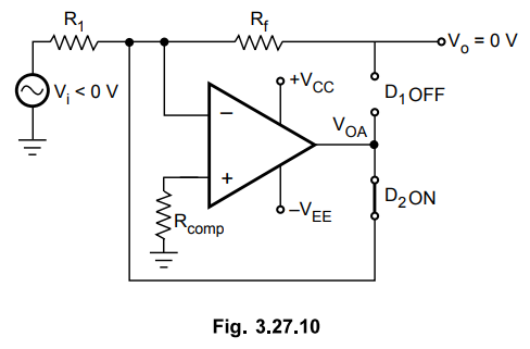
When
Vi < 0 V, immediately VOA becomes highly positive due
to which D2 becomes forward biased and Df reverse biased. As D1is
OFF; Vo = 0 V while diode D2 prevents op-amp to go into
the positive saturation. The circuit is shown in the Fig. 3.27.10.
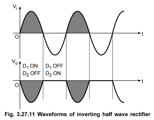
Key
Point As negative half cycle is produced for positive
half cycle of the input, the circuit is called the inverting half wave
rectifier.
The
waveforms are shown in the Fig. 3.27.11.
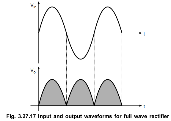
2. Precision Full Wave Rectifiers
The
full wave rectifier circuits accept an a.c. signal at the input, inverts either
the negative or the positive half, and delivers both the inverted and
non-inverted halves at the output, as shown in the Fig. 3.27.12.
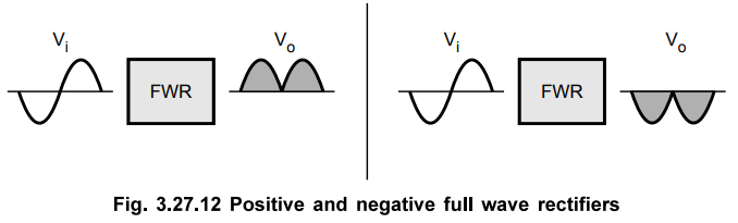
The
operation of the positive full wave rectifier is expressed as,
Vo
= | Vi | ... (3.27.2)
And
that of the negative rectifier as
Vo
= | Vi | ...(3.27.3)
Looking
at equations (3.27.1) and (3.27.2) we can say that precision full wave
rectifier circuits are precision absolute value circuits. Fig. 3.27.13 shows a
full wave rectifier or absolute value circuit.
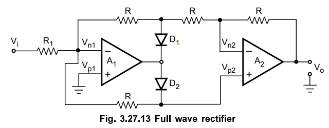
CASE
1 : V; > 0 : When Vi > 0, inverting
side of A1 will force its output to swing negative, thus forward
biasing D1 and reverse biasing D2. Since no current flows
through resistance R connected between Vn1 and Vp2, both
are equipotential.
i.e.
Vn1 = Vp2 = 0V
The
Fig. 3.27.14 shows the equivalent circuit.
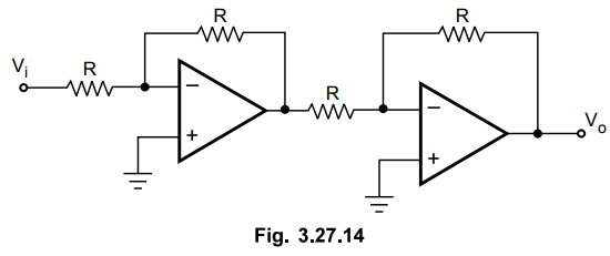
From
equivalent circuit, the output voltage can be given as,
Vo
= (-R / R) – (R / R) Vi = Vi ….. (3.27.4)
CASE
2 :
Vi < 0 : When Vi < 0, negative, the output voltage
of A1 swings to positive, making diode D1 reverse biased and diode D2
forward biased.
The
Fig. 3.27.15 shows the equivalent circuit.
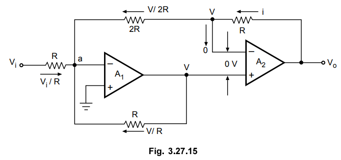
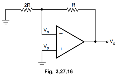
Let
the output voltage of op-amp A1 be V. Smce the differential input to A 2 is
zero, the inverting input terminal is also at voltage V, as shown in the Fig.
3.27.15.
Applying
KCL at node 'a' we have
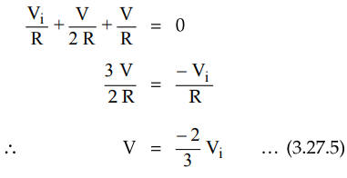
To
find Vo interms of V we concentrate on the equivalent circuit of A2, as shown
in the Fig. 3.27.16.
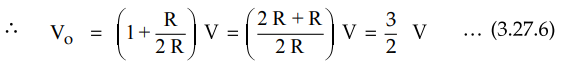
Substituting
value of V in above equation we get,
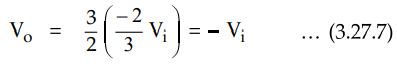
Hence
for Vi < 0 the output is positive. This is illustrated in Fig.
3.27.17.
Review Questions
1. Explain the need of
precision rectifiers.
2. Draw the circuit
and explain the working of precision half wave positive rectifier.
3. Draw the circuit
and explain the working of precision half wave negative rectifier.
4. Draw the circuit
and explain the working of precision full wave rectifier.
Linear Integrated Circuits: Unit III: Applications of Op-amp : Tag: : Working Principle, Pulse, Circuit Diagram | Operational amplifier - Precision Rectifiers using Op-amp
Related Topics
Related Subjects

Linear Integrated Circuits
EE3402 Lic Operational Amplifiers 4th Semester EEE Dept | 2021 Regulation | 4th Semester EEE Dept 2021 Regulation