Digital Logic Circuits: Unit IV: (c) Introduction to Programmable Logic Devices
PROM (Programmable Read Only Memory)
Construction, Principle of Operation
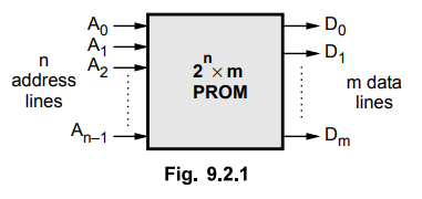
It consists of n-input lines and m-output lines. Each bit combination of the input variables is called an address.
PROM (Programmable Read Only Memory)
•
The Fig. 9.2.1 shows the block diagram of PROM. It consists of n-input lines
and m-output lines. Each bit combination of the input variables is called an
address. Each bit combination that comes out of the output lines is called a
word. The number of bits per word is equal to the number of output lines, m.
The address specified in binary number denotes one of the minterms of n
variables. The number of distinct addresses possible with n-input variables is
2n. An output word can be selected by a unique address and since there are 2n
distinct addresses in PROM, there are 2n distinct words in the PROM. The word
available on the output lines at any given time depends on the address value applied
to the input lines.
•
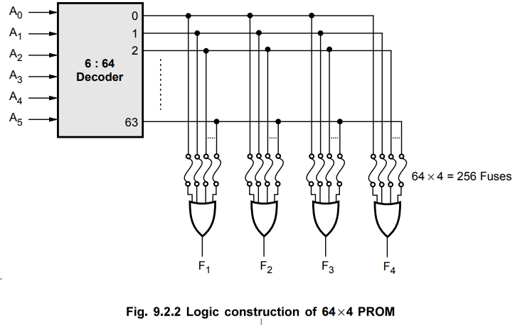
Let us consider 64 × 4 PROM. The PROM consists of 64 words of 4-bits each. This
means that there are four output lines and particular word from 64 words
presently available on the output lines is determined from the six input lines.
There are only six inputs in a 64 × 4 PROM because 26 = 64 and with six
variables, we can specify 64 addresses or minterms. For each address input,
there is a unique selected word. Thus, if the input address is 000000, word number
0 is selected and applied to the output lines. If the input address is 111111,
word number 63 is selected and applied to the output lines.
•
The Fig. 9.2.2 shows the internal logic construction of a 64 × 4 PROM. The six
input variables are decoded in 64 lines by means of 64 AND gates and 6
inverters. Each output of the decoder represents one of the minterms of a
function of six variables. The 64 outputs of the decoder are connected through
fuses to each OR gate. Only four of these fuses are shown in the diagram, but
actually each OR gate has 64 inputs and each input goes through a fuse that can
be blown as desired.
•
The PROM is a two level implementation in sum of minterms form. Let us see
AND-OR and AND-OR-INVERTER implementation of PROM. Fig. 9.2.3 shows the 4 × 2
PROM with AND-OR and AND-OR-INVERTER implementations.

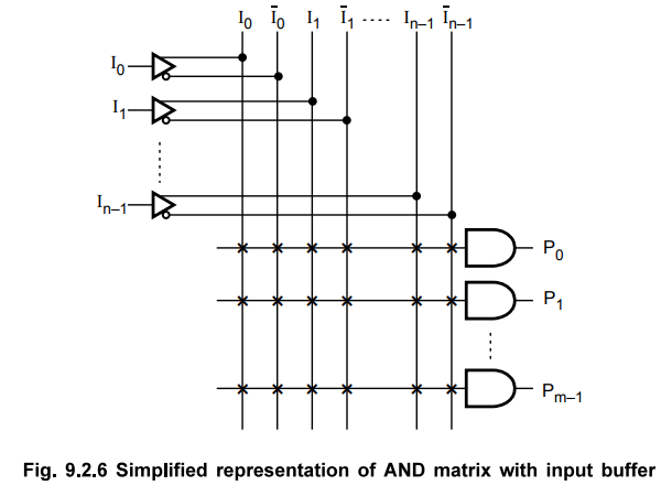
1. AND Matrix
•
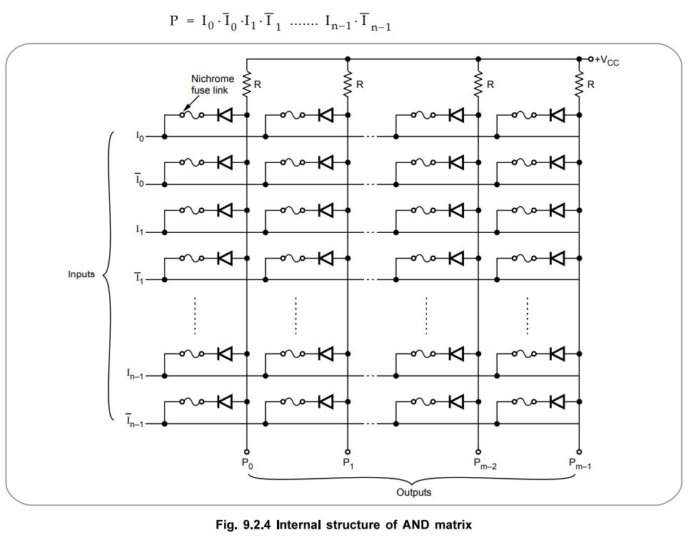
The Fig. 9.2.4 shows the AND matrix. It is used to form product terms. It has m
AND gates with 2n-inputs and m-outputs, one for each AND gate. The Fig. 9.2.4
shows the AND gates formed by diodes and resistors structure. Each AND gate has
all the input variables in complemented and uncomplemented form. There is a
nichrome fuse link in series with each diode which can be bum out to disconnect
particular input for that AND gate. Before programming, all fuse links are
intact and the product term for each AND gate is given by
•
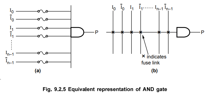
The Fig. 9.2.5 shows the simplified and equivalent representation of input
connections for one AND gate. The array logic symbol shown in Fig. 9.2.5 (b)
uses a single horizontal line connected to the gate input and multiple vertical
lines to indicate the individual inputs. Each intersection between horizontal
line and vertical line indicates the fuse connection.
•
The Fig. 9.2.6 shows the simplified representation of AND matrix with input
buffer.
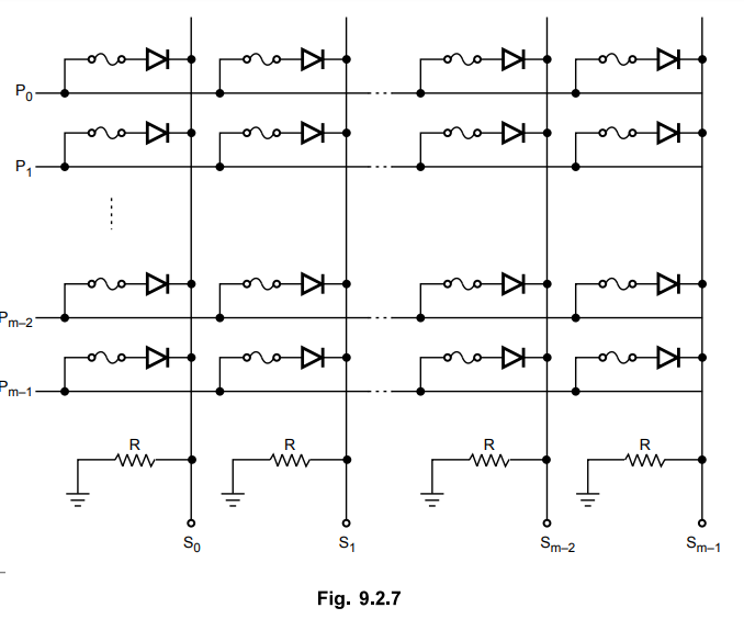
2. OR Matrix
•
The OR matrix is provided to produce the logical sum of the product term
outputs of the AND matrix. The Fig. 9.2.7 shows the OR gates formed by diodes
and resistors structure. Each OR gate has all the product terms as input
variables. There is a nichrome fuse link in series with each diode which can be
bum out to disconnect particular product term for that OR gate. Before
programming, all fuse link in OR matrix are also intact and the sum term for
each OR gate is given by,
•
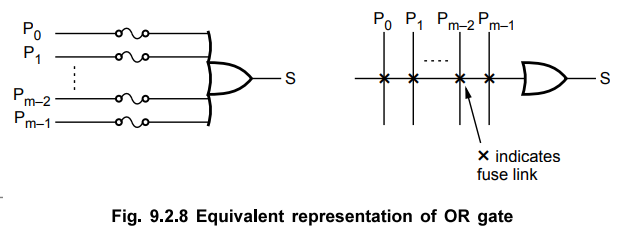
The Fig. 9.2.8 shows the simplified and equivalent representation of input
connections for one OR gate.
•
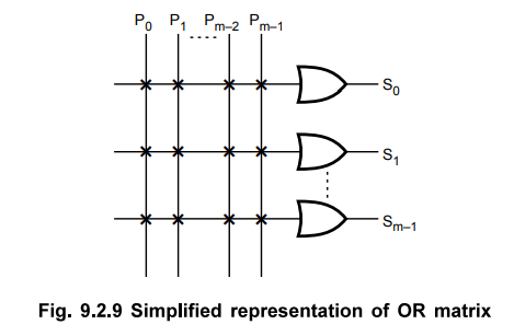
The Fig. 9.2.9 shows the simplified representation of OR matrix.
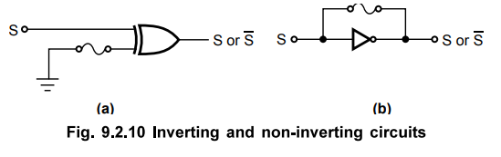
3. Invert / Non-invert Matrix
•
Invert/Non-invert matrix provides output in the complement or uncomplemented
form. The user can program the output in either complement or uncomplement form
as per design requirements. The typical circuits for invert/non-invert matrix
is
as shown in Fig. 9.2.10. In both the cases if fuse is intact the output is in
its uncomplemented form; otherwise output is in the complemented form.
4. Combinational Logic Implementation using PROM
•
Looking at the logic diagram of the PROM, we can realize that each output
provides the sum of all the minterms of n-input variables. We know that any
Boolean function can be expressed in sum of minterms form. By breaking the
links of those minterms not included in the function, each PROM output can be
made to represent the Boolean function of one of the output variables in the
combinational circuit. For an n-input, m-output combinational circuit, we need
a 2n × m PROM.
Examples
for Understanding
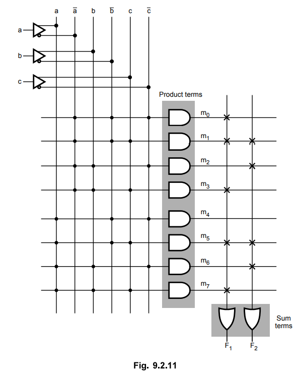
Ex.
9.2.1 Using PROM realize the following expressions.
F1
(a, b, c) = ∑ m (0, 1, 3, 5, 7)
F2
(a, b, c) = ∑ m (1, 2, 5, 6)
Sol.
:
The given functions have three inputs. They generate 23 = 8 minterms
and since there are two functions, there are two outputs. The functions can be
realized as shown in Fig. 9.2.11.
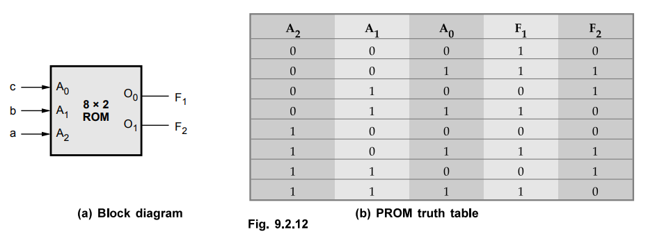
The
Fig. 9.2.12 shows the block diagram and truth table of PROM.
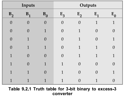
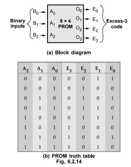
Ex.
9.2.2 Design a combinational using a PROM. The circuit accepts 3-bit binary
number and generates its equivalent Excess-3 code.
Sol. : Let us derive the truth table for the given combination circuit. Table 9.2.1 shows the truth table.
• In practice when we are designing combinational circuits with PROM, it is not necessary to show the internal gate connections of fuses inside the unit, as shown in the Fig. 9.2.13.
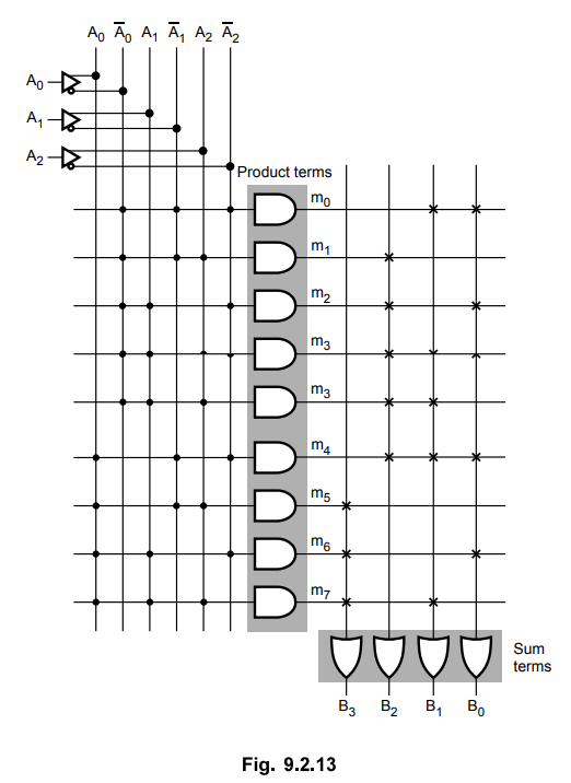
This was shown for demonstration purpose only. The
designer has to only specify the PROM (inputs and outputs) and its truth table,
as shown in the Fig. 9.2.14.
Examples
with Solutions
Ex.
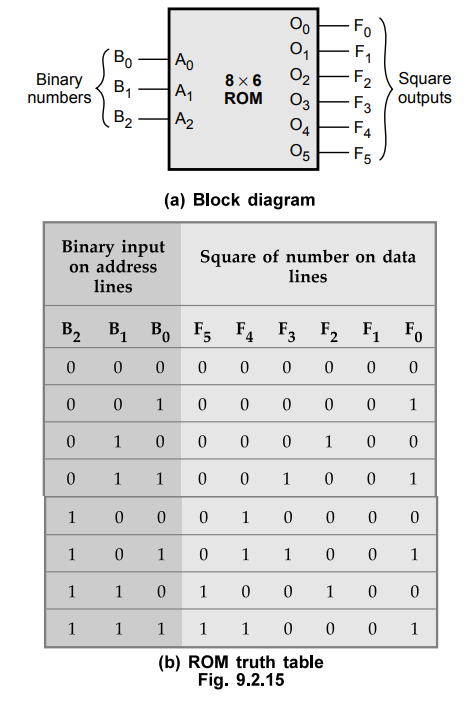
9.2.3 Design a combinational circuit using ROM. The circuit accepts 3-bit
number and generates an output binary number equal to square of input number.
AU
: May-10, Marks 16
Sol.
Ex.
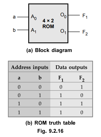
9.2.4 Design ROM for the following functions
F1
= ∑ (1,2,3); F2 = ∑ (0,2)
Sol.
:
The given functions have 4 minterms. To generate four minterms and two outputs
we need 4 x 2 ROM. For 4x2 ROM, there are two address inputs and two data
outputs.
Examples
for Practice
Ex.
9.2.5 Design a switching circuit that converts a 4 bit binary code into a 4 bit
Gray code using ROM array.
Ex. 9.2.6 Design a 3-bit gray to binary code converter using suitable ROM.
Review Questions
1. What is PROM ?
2. Explain the logic construction of a typical PROM.
Digital Logic Circuits: Unit IV: (c) Introduction to Programmable Logic Devices : Tag: : Construction, Principle of Operation - PROM (Programmable Read Only Memory)
Related Topics
Related Subjects

Digital Logic Circuits
EE3302 3rd Semester EEE Dept | 2021 Regulation | 3rd Semester EEE Dept 2021 Regulation