Electron Devices and Circuits: Unit IV: Multistage and Differential Amplifiers
Push Pull Class B Power Amplifier
Operation of the circuit, Equivalent circuit, Calculation, Advantages, Disadvantages
• The push pull circuit requires two transformers, one as input transformer called driver transformer and the other to connect the load called output transformer.
Push Pull Class B Power Amplifier
•
The push pull circuit requires two transformers, one as input transformer
called driver transformer and the other to connect the load called output
transformer.
• Both the transformers are centre tapped transformers. The push pull class B amplifier circuit is shown in the Fig. 8.17.1.

•
In the circuit, both Qx and Q2 transistors are of n-p-n type.
•
The circuit can use both Q1 and Q2 of p-n-p type. In such a case, the only
change is that the supply voltage must be - VCC, the basic circuit remains the
same.
•
The input signal is applied to the primary of the driver transformer.
•
The centre tap on the secondary of the driver transformer is grounded.
•
The centre tap on the primary of the output transformer is connected to the
supply voltage + V
• With respect to the centre tap, for a positive half cycle of input signal, the point A shown on the secondary of the driver transformer will be positive. While the point B will be negative.
•
Thus the voltages in the two halves of the secondary of the driver transformer
will be equal but with opposite polarity.
•
Hence the input signals applied to the base of the transistors Q1
and Q2 will be 180° out of phase.
Operation
of the circuit :
•
For positive half cycle of the input, A is positive and B is negative.
•
Due to this, Q1 gets driven into active region while Q2 is cut-off.
•
Thus ib1 flows while i b2 = 0, as shown in the Fig.
8.17.2.
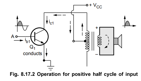
• Hence icl flows through upper part of
primary of the output transformer while ic2 =0.
•
Thus positive half cycle is produced across the load.
•
For negative half cycle of the input, B is positive and A is negative.
• Due to this, Q2 gets driven into active
region while Q1 is cut-off.
•
Thus ib2 flows while iM = 0 as shown in the Fig. 8.17.3.
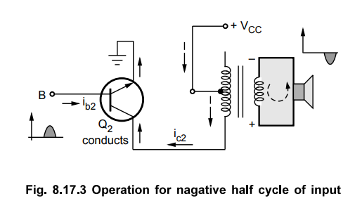
•
Hence ic2 flows through lower part of primary of the output
transformer while ic1 = 0.
•
Thus negative half cycle is produced across the load.
•
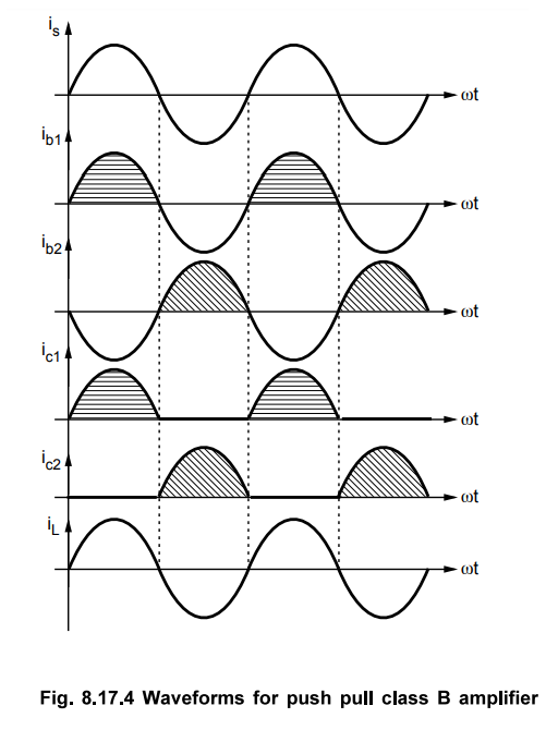
The full cycle is thus obtained across the load for full input cycle.
•
The waveforms of the input current, base currents, collector currents and the
load current are shown in the Fig. 8.17.4.
Important
Concept
For
the output transformer, the number of the turns of each half of the primary is
N1 while the number of the turns on the secondary is N2.
Hence the total number of primary turns is 2N1. So turns ratio of
the output transformer is specified as 2N2 : N2.
1. D.C. Operation
•
The d.c. biasing point i.e. Q point is adjusted on the X-axis such that VCEQ
= VCC and ICEQ is zero.
•
Hence the co-ordinates of the Q point are (VCC, 0). There is no d.c. base bias
voltage.
2. D.C. Power Input
•
Each transistor output is in the form of half rectified waveform.
•
Hence if Im is the peak value of the output current of each transistor, the
d.c. or average value is 1m due to half rectified waveform.
•
The two currents, drawn by the two transistors, form the d.c. supply are in the
same direction. Hence the total d.c. or average current drawn from the supply
is the algebraic sum of the individual average current drawn by each
transistor.

3. AC Operation
•
When a.c. signal is applied to the driver transformer, for positive half cycle
of input Q1 conducts while for negative half cycle of input Q2 conducts.
•
When Qi conducts, lower half of the primary of the output transformer does not
carry any current. Hence only N1 number of turns carry the current.
•
While when Q2 conducts, upper half of the primary does not carry any current.
Hence again only N number of turns carry the current. Hence the reflected load
on the primary can be written as,

•
Though the turns ratio is 2N1 : N2, while operation the
ratio becomes n=N2 / N1 which decides the reflected load.
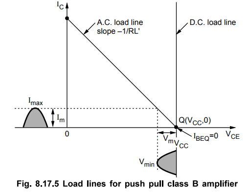
•
The slope of the a.c. load line is -1/RL while the d.c. load line is the
vertical line passing through the operating point Q on the X-axis. The load
lines are shown in th Fig. 8.17.5.
•
The slope of the a.c. load line (magnitude of slope) can be represented interms
of Vm and Im as,
where
Im = Peak value of the collector current
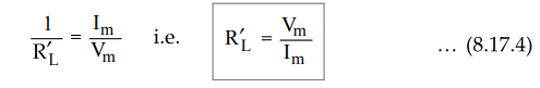
4. A.C. Power Output
•
As Im and Vm are the peak values of the output current and the output voltage
respectively, then
Vrms
= Vm / √2 and Irms = Im / √2
•
Hence the a.c. power output is expressed as,

•
While using peak values it can be expressed as,

5. Efficiency
•
The efficiency of the class B amplifier can be calculated using the basic
equation.

6. Maximum Efficiency
•
From the equation (8.17.7), it is clear that as the peak value of the collector
voltage Vm increases, the efficiency increases.
•
The maximum value of Vm possible is equal to VCC as shown in the Fig. 8.17.6.
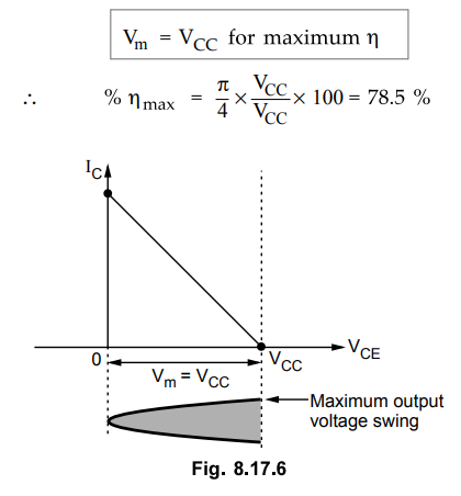
Important
Concept
Thus
the maximum possible theoretical efficiency in case of push pull class B
amplifier is 78.5 % which is much higher than the transformer coupled class A
amplifier.
For
practical circuits it is upto 65 to 70 %.
Important
Concept
Practically
the collector-emitter voltage of transistor is neglected as small. But if VCE(min)
is given then maximum collector voltage Vm reduces by VCE
min and becomes Vm = VCC - VCE (min)
under maximum efficiency condition.
7. Advantages
1.
The efficiency is much higher than the class A operation.
2.
When there is no input signal, the power dissipation is zero.
3.
The even harmonics get cancelled. This reduces the harmonic distortion.
4.
As the d.c. current components flow in opposite direction through the primary
winding, there is no possibility of d.c. saturation of the core.
5.
Ripples present in supply voltage also get eliminated.
6.
Due to the transformer, impedance matching is possible.
8. Disadvantages
1.
Two centre tap transformers are necessary.
2.
The transformers, make the circuit bulky and hence costlier.
3.
Frequency response is poor.
Review Questions
1. Draw the circuit diagram of a class B push-pull power
amplifier and discuss its operation, merits and demerits.
2. Find out the expressions for the following parameters for the
class B push-pull amplifier :
i) d.c. power input ii) a.c. power output iii) efficiency iv)
maximum efficiency v) power dissipation.
3. Show that the maximum conversion efficiency of the ideal
class B push-pull circuit is 78.5 %.
4. Explain with circuit diagram class B power amplifier and
derive for its efficiency.
AU : Dec.-15, Marks 8
Electron Devices and Circuits: Unit IV: Multistage and Differential Amplifiers : Tag: : Operation of the circuit, Equivalent circuit, Calculation, Advantages, Disadvantages - Push Pull Class B Power Amplifier
Related Topics
Related Subjects

Electron Devices and Circuits
EC3301 3rd Semester EEE Dept | 2021 Regulation | 3rd Semester EEE Dept 2021 Regulation