Microprocessors and Microcontrollers: Unit IV: (f) A/D and D/A Converter Interfacing with 8085
Sample and Hold Circuit and Multiplexer
A/D and D/A Converter Interfacing with 8085
A sample and hold circuit is used to interface real-world signals. The purpose of this circuit is to hold the analog value steady for a short time while the converter or other following system performs some operation that takes a little time.
Sample and Hold Circuit and Multiplexer
AU
: May-04, 05, Dec.-05
A
sample and hold circuit is used to interface real-world signals. The purpose of
this circuit is to hold the analog value steady for a short time while the
converter or other following system performs some operation that takes a little
time.
For
accurate analog to digital conversion the analog input voltage should be held
constant during the conversion cycle. If the analog input voltage changes by
more than ± 1/2 LSB an error can occur in the digital output code. To
illustrate the effect of a changing analog input voltage on the conversion
processor, let us consider a situation of a successive approximation ADC with
an analog input voltage that is initially zero, but there happen to be a large
change in voltage amplitude occurring during the conversion process. Fig. 13.9.1
shows the changing input voltage and its effect on the successive approximation
conversion process.

As shown in Fig. 13.9.1 analog input voltage at start of conversion process is zero volts and at the end of conversion process it is near to 1.5 volts, and the conversion process result is 0102, i.e. 2.5 V. This result does not corresponds to the analog voltage at the start of conversion or at the end of conversion. To minimise the occurrence of these errors it is necessary to hold the value of the analog input voltage constant during the conversion process. The sample and hold circuit does this task.
As
its name implies, the sample and hold (S/H) circuit samples the value of the
input signal in response to a sampling command and hold it at the output until
arrival of the next command.
It
samples an analog input voltage in a very short period, generally in the range
of 1 to 10 µs, and holds the sampled voltage level for an extended period,
which can range from a few millisecond to several seconds. Fig. 13.9.2(b) shows
input and output response of the sample and hold circuit.
The
sample and hold circuit uses to basic components analog switch and capacitor.
The Fig. 13.9.2(a) shows the basic sample and hold circuit. The circuit tracks
the analog signal until the sample command causes the digital switch to isolate
the capacitor from the signal, and the capacitor holds this analog voltage
during A/D conversion.

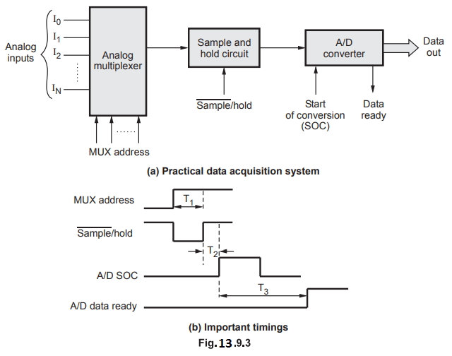
The
Fig. 13.9.3(a) illustrates a practical data acquisition system using an analog
multiplexer, a sample and hold circuit and an A/D converter. In such system, microprocessor
selects one of the input channels through multiplexer address lines. When the  / hold signal is low, the sample and hold circuit tracks the analog input;
otherwise the sample and hold circuit holds the analog input. The stable analog
signal is then converted into its digital equivalent using A/D converter.
Microprocessor reads this output using input port.
/ hold signal is low, the sample and hold circuit tracks the analog input;
otherwise the sample and hold circuit holds the analog input. The stable analog
signal is then converted into its digital equivalent using A/D converter.
Microprocessor reads this output using input port.
1. Data Acquisition System using 8085
The
Fig. 13.9.4 shows the data acquisition system using 8085 and 8255. Here 8255 is
used to generate required control signals and accept data from A/D converter.
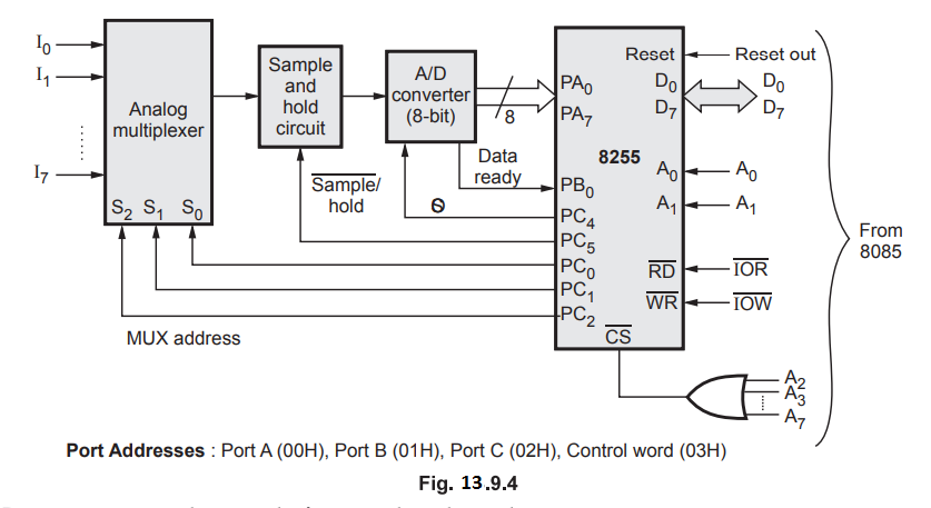
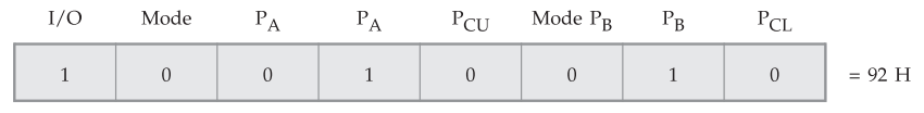
According
to ports used we require to configure 8255 as follows :
•
Port A : input (mode 0)
•
Port B : input (mode 0)
•
Port C : output
Control
Word
Program
:
To take from analog channel 2.
MVI
A, 92H ; Configure 8255 by
OUT
03H ; Sending control word to control register
MVI
A, 22H ; Send MUX address, make /hold
OUT
02H ; line HIGH and make SOC low
MVI
A, 0AH ; Make /hold Low using BSR mode
OUT
03H
MVI
A, 0BH ; Make /hold High using BSR mode
OUT
03H
MVI
A, 09H ; Make SOC High using BSR mode
OUT
03H
MVI
A, 08H ; Make SOC low using BSR
mode
OUT
03H
BACK
: IN 01H ; Read port B
ANI
01H ; Check PB0
JZ
Back ; if zero wait for Data Ready
IN
00H ; Read data through port A
HLT
; Stop
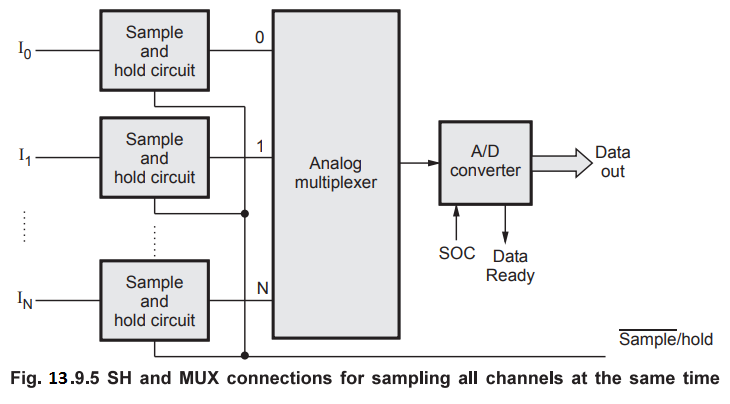
2. Another Way of Connecting MUX and SH Circuits
In
the previous examples we have seen that sample and hold circuit is connected after
the multiplexer. Here, we have to select analog signal turn by turn and then
sample it. Thus, we can not sample all the channels at the same time. If it is
required to read values from all the channels at the same time then we need
separate sample and hold circuit for each channel. This is illustrated in Fig.
13.9.5. With this configuration we can sample analog signals from all channels
at a time. The microprocessor then selects channel one by one and read the
respective values one by one with the help of multiplexer and A/D converter.
Review Questions
1. What is sample and
hold circuit ? Explain the purpose of it.
2. Explain the use of
sample and hold circuit with multiplexer.
3. Draw and explain
the data acquisition system.
4. Draw and explain
the operation of a sample and hold circuit. AU : May-04,05, Marks
4
5. Explain the sample
and hold IC.
AU : Dec.-05, Marks 12
Microprocessors and Microcontrollers: Unit IV: (f) A/D and D/A Converter Interfacing with 8085 : Tag: : A/D and D/A Converter Interfacing with 8085 - Sample and Hold Circuit and Multiplexer