Linear Integrated Circuits: Unit III: Applications of Op-amp
Sample and Hold Circuit using Op-amp
Working Principle, Circuit Diagram, Advantages, Applications | Operational amplifier
It samples an analog input voltage in a very short period, generally in the range of 1 to 10 ps, and holds the sampled voltage level for an extended period, which can range from a few millisecond to several seconds.
Sample and Hold Circuit
As
its name implies, the sample and hold (S/H) circuit samples the value of the
input signal in response to a sampling command and hold it at the output until
arrival of the next command. It samples an analog input voltage in a very short
period, generally in the range of 1 to 10 ps, and holds the sampled voltage
level for an extended period, which can range from a few millisecond to several
seconds. Fig. 3.24.1 shows input and output response of the sample and hold
circuit.

The
sample and hold circuit uses to basic components analog switch and capacitor.
The Fig. 3.24.2 shows the basic sample and hold circuit.
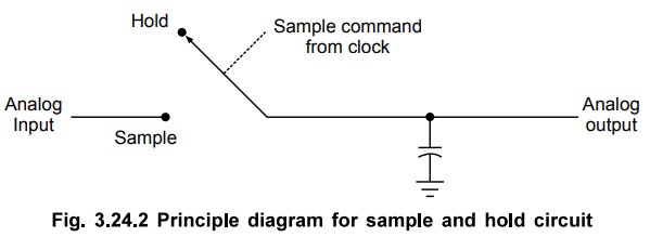
The circuit tracks the analog signal until the sample command causes the digital switch isolate the capacitor from to the signal, and the capacitor holds this analog voltage during A/D conversion.
Sample and Hold Circuits
Four
basic sample and hold circuits are shown in Fig. 3.24.3. In these circuits a
JFET is used as switch. During the sampling time the JFET switch is turned on,
and the holding capacitor charges up to the level of the analog input voltage.
At the end of this short sampling period, the JFET switch is turned off. This
isolates the holding capacitor CH from the input signal. As a
result, the voltage across capacitor CH and hence the output voltage
will remain essentially constant at the value of the input voltage at the end
of the sampling time. However, there will be a small drop-off or drop of the
capacitor voltage during the hold period due to the various leakage currents.
To avoid this, input and output buffers (voltage follower) circuits are used.
Fig.
3.24.3 (a) shows the open loop architecture of the sample and hold circuit.
Remaining figures show the closed loop architecture of the sample and hold
circuit. Open loop type sample and hold circuits are faster than closed loop
types which have delayed output feedback to the input buffer. However, closed
loop architectures provide higher dc accuracy because of this feedback,
cancelling the output amplifier offset errors.
The
acquisition time of a S/H circuit is the time required for the holding
capacitor CH to charge up to a level close to the input voltage during
sampling. The acquisition time for S/H circuit should be as low as possible. In
the circuit of Fig. 3.24.3 (a) there are three principle factors that will
control the acquisition time. These factors are :
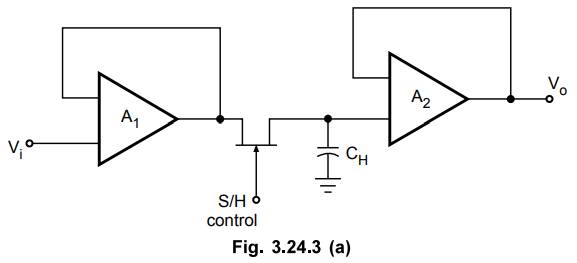
•
RC time constant where R is the rds (ON), i.e. on resistance of JFET
and C is the holding capacitance CH
•
Maximum output current, which can be source or sunk by the operational
amplifier.
•
Slew rate of the op-amp. The circuit shown in Fig. 3.24.3 (b) V° offers some
advantage over that of Fig. 3.24.3 (a) in terms of the acquisition time since
the rds (ON) of the JFET switch is inside the feedback loop of A i and A 2.
Therefore the acquisition time for this circuit is limited by maximum output
current and slew rate of the op-amp, rather than the RC time constant.
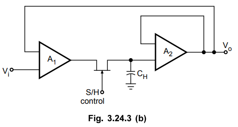
The
S/H circuit of Fig. 3.24.3 (c) performs in a fashion similar to that of Fig.
3.24.3 (b) but it offers the additional feature of providing voltage gain. The
voltage gain of this circuit can be given as A = 1 + (RF/R1).
Therefore, the sampled output voltage is equal to the sampled input voltage
multiplied by the voltage gain factor 1 + (RF/R1).
The
S/H circuit of Fig. 3.24.3 (d) offers two advantages. The faster capacitor
charging rate provides shorter acquisition time. This is because the voltage at
the inverting input terminal of A2 is equal to the capacitor voltage
divided by the open loop gain of A2. In this circuit, the summing
input of A2 remains at virtual ground. Due to this, the charge removed from the
summing junction via Cgd is constant regardless of the input and output signal
levels. This removed charge appears as a constant offset at the output.
However, as it is constant, it can be nulled by any standard offset trimming
technique.

1. Advantages of Sample and Hold Circuits
1.
The primary use of the sample and hold circuit to hold the sampled analog input
voltage constant during conversion time of A/D converter.
2.
In case of multichannel ADCs, synchronization can be achieved by sampling
signals from all channels at the same time.
3.
It also reduces the crosstalk in the multiplexer.
2. Applications of Sample and Hold Circuits
The
applications of such sample and hold circuit are :
i)
Digital interfacing.
ii)
Analog to digital converter circuits.
iii)
Pulse modulation systems.
iv)
In storage of outputs of a multiplexer between updates in data distribution
systems.
v)
In reset-stabilised op-amps.
vi)
In analog demultiplexers.
Review Question
1. Explain the working of sample/hold circuit.
Linear Integrated Circuits: Unit III: Applications of Op-amp : Tag: : Working Principle, Circuit Diagram, Advantages, Applications | Operational amplifier - Sample and Hold Circuit using Op-amp
Related Topics
Related Subjects

Linear Integrated Circuits
EE3402 Lic Operational Amplifiers 4th Semester EEE Dept | 2021 Regulation | 4th Semester EEE Dept 2021 Regulation