Electron Devices and Circuits: Unit IV: Multistage and Differential Amplifiers
Single Tuned Amplifiers
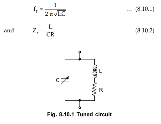
• To amplify the selective range of frequencies, the resistive load, Rc is replaced by a tuned circuit. The tuned circuit is capable of amplifying a signal over a narrow band of frequencies centered at fr.
Single Tuned Amplifiers
AU
: Dec.-04, 05, 06, 07, 08, 09, 10, 11, 12, 15 May-03,04, 05, 06, 07, 09, 11,
12, 13
1. Introduction
•
To amplify the selective range of frequencies, the resistive load, Rc is
replaced by a tuned circuit. The tuned circuit is capable of amplifying a
signal over a narrow band of frequencies centered at fr. The amplifiers with
such a tuned circuit as a load are known as tuned amplifier. Since tuned amplifiers
amplify narrow band of frequencies they are also known as narrow band
amplifiers. In the timed RF amplifiers the center frequency may range from 1 to
many megahertz and side frequencies extend to 5 or 10 kHz for amplitude
modulated voice or music and to several hundred kilohertz for other
amplifications.
•
The Fig. 8.10.1 shows the tuned parallel LC circuit which resonates at a
particular frequency. The resonance frequency and impedance of tuned circuit is
given as,
•
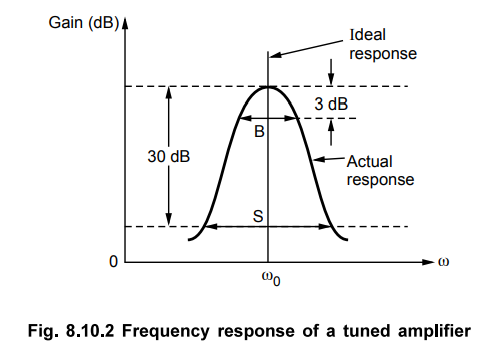
The response of tuned amplifiers is maximum at resonant frequency and it falls
sharply for frequencies below and above the resonant frequency, as shown in the
Fig. 8.10.2. It is designed to reject all frequencies below a lower cutoff
frequency, fL and above a upper cut-off frequency fH’
•
As shown in the Fig. 8.10.2, 3 dB bandwidth is denoted as B and 30 dB bandwidth
is denoted as S. The ratio of the 30 dB bandwidth (S) to the 3 dB bandwidth (B)
is known as skirt selectivity.
•
At resonance, inductive and capacitive effects of tuned circuit cancel each
other. As a result, circuit is like resistive and cos $ = 1 i.e. voltage and
current are in phase. For frequencies above resonance circuit is like
capacitive and for frequencies below resonance it is like inductive. Since
tuned circuit is purely resistive at resonance it can be used as a load for
amplifier.
a.
Coll Losses
•
As shown in Fig. 8.10.1, the timed circuit consists of a coil. Practically,
coil is not purely inductive. It consists of few losses and they are
represented in the form of leakage resistance in series with the inductor. The
total loss of the coil is comprised of copper loss, eddy current loss and
hysteresis loss. The copper loss at low frequencies is equivalent to the d.c.
resistance of the coil. Copper loss is inversely proportional to frequency.
Therefore, as frequency increases, the copper loss decreases. Eddy current loss
in iron and copper coil are due to currents flowing within the copper or core
cased by induction. The result of eddy currents is a loss due to heating within
the inductors copper or core. Eddy current losses are directly proportional to
frequency. Hysteresis loss is proportional to the area enclosed by the
hysteresis loop and to the rate at which this loop is transversed. It is a
function of signal level and increases with frequency. Hysteresis loss is
however independent of frequency.
•
As mentioned earlier, the total losses in the coil or inductor is represented
by inductance in series with leakage resistance of the coil. It is as shown in
Fig. 8.10.3.

b.
Q Factor
•
Quality factor (Q) is important
characteristics of an inductor. The Q is the ratio of reactance to resistance
and therefore it is unitless. It is the measure of how 'pure' or 'real' an
inductor is (i.e. the inductor contains only reactance). The higher the Q of an
inductor the fewer losses there are in the inductor. The Q factor also can be
defined as the measure of efficiency with which inductor can store the energy.
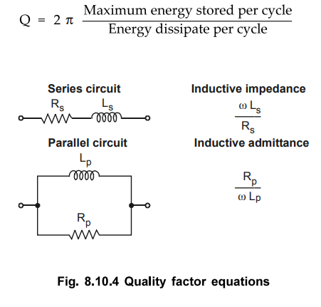
•
The dissipation factor (D) that can be referred to as the total loss within a
component is defined as 1/Q. The Fig. 8.10.4 shows the quality factor equations
for series and parallel circuits and its relation with dissipation factor.
Quality
factor equation Q = 1/D = ωLs / Rs = Rp / ωLp
Ex.
8.10.1 Derive the expression for quality factor, Q of an inductor.
Sol.
:
Consider a circuit shown in the Fig. 8.10.5. Here, a sinusoidal voltage Vmsin
rot is applied to the inductor with an internal resistor Rs.
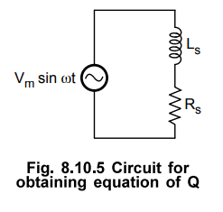
The
maximum energy stored per cycle = 1/2 I2m Ls … (1)
and
Average
power dissipated per cycle = ( Im / √2)2 Rs
Energy
= power × Time
Average
energy dissipated in the inductor per cycle
=
Power × Priiodic time for one cycle = Power × T = ( Im / √2)2
Rs × T
=
( Im / √2)2 Rs × 1/f T = 1/f
=
I2mRs / 2f
Substituting
equation (1) and (2) in the equation of Q. We have,

Ex.
8.10.2 Derive the expression for Q-factor of a capacitor.
Sol.
:
1.
Capacitor with a small resistor in series
•
Consider a circuit shown in Fig. 8.10.6. Here, a sinusoidal voltage Vm sin oot
is applied to the capacitor with a small resistor.
•
Maximum energy stored in the capacitor per cycle = 1/ 2 Cs V2max
where
Vmax = Im / ωCs when Rs >> 1 / ωCs
Maximum
energy stored in the capacitor per cycle = 1/2 CV2max = I2m / 2 ω2Cs
Energy
dissipated per cycle = I2m Rs / 2f
Substituting
equation (1) and (2) in the equation of Q. We have,
2.
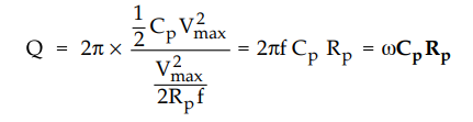
Capacitor with a high resistor in parallel
•
Consider a circuit shown in Fig. 8.10.7. Here, a sinusoidal voltage
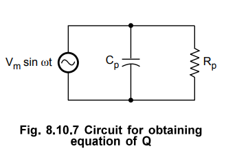
Vm
sin ωt is applied to the capacitor with a high resistor in parallel.
Maximum
energy stored in the capacitor = 1/2 CV2max … (3)
Average
power dissipated per cycle in Rp = (Vmax/√2)2 × 1/Rp
= V2max/2 Rp
Energy
dissipated per cycle = V2max/2 Rp × T = V2max/2
Rpf T = 1/f
Substituting
equation (3) and (4) in the equation of Q we have,
c.
Unloaded and Loaded Q
•
When the tank circuit is not connected to any external circuit or load, Q
accounts for the internal losses and it is known as unloaded quality factor,
Qv. It is defined as,
QU
= 2π × Maximum energy stored per cycle / Energy dissipated per cycle in tank
circuit
•
In practice, the tank circuit is connected to the load. Hence, the energy
dissipation takes place in the tank circuit as well as in the external load.
The loaded quality factor, QL is defined as
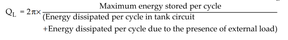
•
Due to the loading, the equivalent parallel resistance Rp is reduced by any external
resistance REXT placed in parallel with the circuit. Therefore, the loaded
Q-factor is given by
QL
= RT / XL = RT / ωLp
where,
RT = Rp || REXT
•
The quality factor QL determines the 3 dB bandwidth for the resonant circuit.
The 3 dB bandwidth for resonant circuit is given as,
BW
= fr / QL
where
fr represents the centre frequency of a resonator and BW represents
the bandwidth.
•
If Q is large, bandwidth is small and circuit will be highly selective. For
small Q values bandwidth is high and selectivity of the circuit is lost, as
shown in the Fig. 8.10.8.
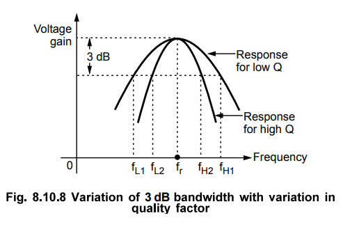
•
Thus in tuned amplifier Q is kept as high as possible to get the better
selectivity. Such tuned amplifiers are used in communication or broadcast
receivers where it is necessary to amplify only selected band of frequencies.
Ex. 8.10.3 A tuned amplifier has its maximum gain at a frequency of 2 MHz and has a bandwidth of 50 kHz. Calculate the Q factor.
Sol.
:
Given : fr = 2 MHz, BW = 50 kHz
We
have Q = fr / BW = 2 × 10⁶ / 50 × 103 = 40
Ex.
8.10.4 A tuned amplifier is designed to receive AM broadcast of speech signal
at 650 kHz. What is needed Q for amplifier?
AU
: ECE : Dec.-09, Marks 2
Sol.
:
Given : fc = 650 kHz
Assume
maximum modulating frequency for AM broadcast speech signal = 3 kHz.
Bandwidth
= 2fm = 2 × 3 = 6 kHz
We
have Q = fr / BW = 650 kHz / 6 kHz =
108.33
d.
Parallel Resonant Circuit
•
The Fig. 8.10.9 shows the tuned parallel LC circuit which resonates at a
particular frequency.
•
The total admittance of the parallel tuned circuit is given by,
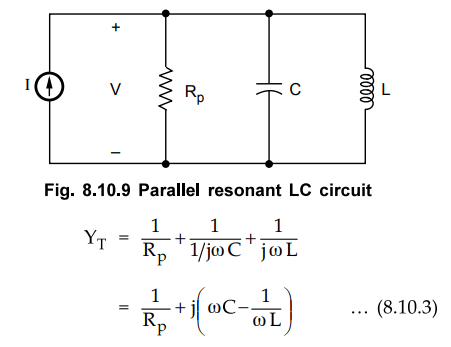
•
At resonance imaginary part is zero, thus equating it to zero we get,

•
In parallel resonant circuit, the voltage V is common to the three circuit elements,
and we can write the maximum energy of the circuit in terms of the capacitance
as C V2m/2. The energy loss per cycle is (V2m/2Rp). p- Then Q is

•
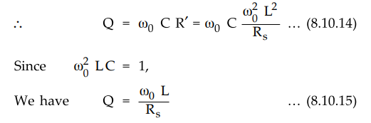
Once the resonant condition is determined by O>-' L C = 1, the value of Q of
a resonant circuit is determined by Rp , or by the ratio of C to L.
•
At resonance, reactive term is equal to zero, therefore,
YT
= 1 / Rp
Impedance
at resonance, Zo = Rp ...
(8.10.7)
•
Using equation (8.10.6) and (8.10.7) we can write
Z0
= Q ω0
L = Q / ω0 C ...(8.10.8)
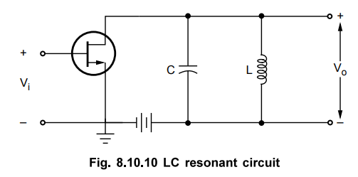
•
The impedance of the resonant circuit is required in determining circuit gain.
The gain of the circuit shown in Fig. 8.10.10 is
Av
= - gm RL = - gm ω0 L (8.10.9)
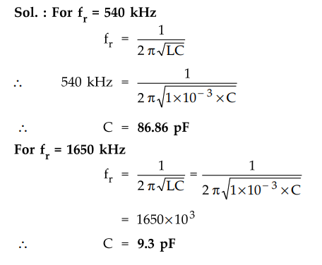
Ex.
8.10.5 A tank circuit contains an inductance of 1 mH. Find out the range of
tuning capacitor value if the resonant frequency ranges from 540 kHz to 1650
kHz.
Ex.
8.10.6 A parallel resonant circuit has an inductance if 150 pH and a
capacitance of 100 pF. Find the resonant frequency.
AU
: ECE : May-07, Marks 2
Sol.
: Given
: L = 150 µH and C = 100 pF
f0
= 1 / 2π√LC = 1 / 2π√150 × 10-6 × 100 × 10-12
=
1299.494 kHz
•
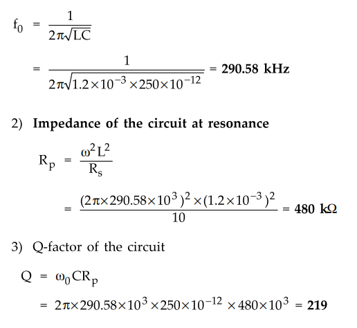
Ex. 8.10.7 A parallel resonant circuit has a capacitor of 250 pF in one branch
and inductance of 1.2 mH and a resistance of 10 Ω in the parallel branch. Find
(1) resonant frequency (2) impedance of the circuit at resonance (3) Q-factor
of the circuit.
Sol.
:
1) Resonant frequency
d.
Series Resonant Circuit
•
The Fig. 8.10.11 (a) shows the series resonant circuit. Here, the loss element
Rs is n sries with L series branch is

•
Usually at high Q conditions, ω2 L2 >> R2a
. Therefore, we can drop term R2a in the denominator to
get
Y
= Rs / ω2 L2 + 1 / jωL
=
1 / R, + 1 / j ωL ... (8.10.11)
•
This equation gives us the parallel arrangement as shown in Fig. 8.10.11 (b),
where R' is given by
R
= ω2 L2 / Rs
... (8.10.12)
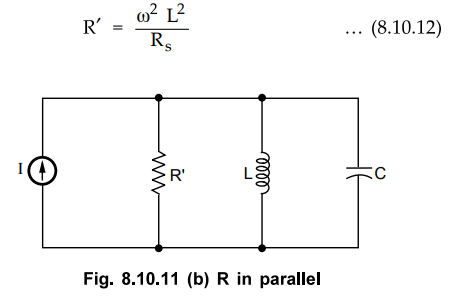
Rs
= ω2 L2 / Rs ... (8.10.13)
•
The equations (8.10.12) and (8.10.13) represent transformations for passing
from the series form of circuit to the parallel form, or vice versa. The
inductance L does not change in the transformations but a small series Rs
transforms to a large R' in parallel with L.
•
In the previous section we have seen that for parallel circuit Q is
Q
= ωo C Rp
•
Here, Rp is represented by R'
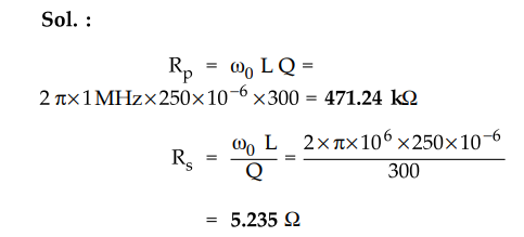
Ex.
8.10.8 An inductor of 250 pH has Q = 300 at 1 MHz. Determine Rg and R of
inductor.
AU
: ECE ; May-06, Dec.-12, Marks 2
Sol.
:
Ex.
8.10.9 A resonant circuit has C = 120 pF, L = 100 µH (with a series resistance
of 5 ohms). Find the Q factor and the bandwidth of the circuit.
AU
: ECE : Dec.-04, Marks 4
Sol.
:
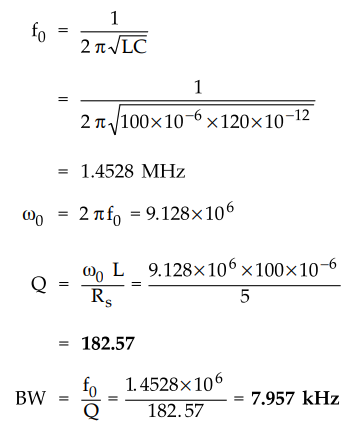
Ex.
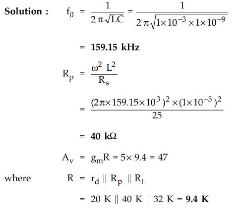
8.10.10 A single tuned amplifier using n channel JFET with gm = 5
mA/V and rd = 20 k Ω, has tank circuit
with L = 1 mH, series resistance of the coil R = 25 Q and C = 1 nF. Calculate
the voltage gain at resonance if RL = 32 k Ω.
AU
: ECE : May-05, Marks 2
Solution
:
Ex.
8.10.11 The drain circuit of a FET tuned radio frequency amplifier has a 100 pF
capacitor placed In parallel with an inductor L, whose unloaded Q-factor is
100. If the frequency of resonance is 1 MHz and the transistor output
resistance is 20 kQ calculate the loaded Q-factor, inductance and loaded bandwidth.
AU
: ECE : Dec.-11, Marks 8
Sol.
:
The total resistive loading on the tuned circuit consists of the transistor
output impedance and the dynamic impedance in parallel R = RsRp/(Rs + Rp). The
dynamic impedance using the unloaded Q-factor is

2. Signal Tuned Transistor Amplifier
•
A common emitter amplifier can be converted into a single tuned amplifier by
including a parallel tuned circuit as shown in Fig. 8.10.12. The biasing
components are not shown for simplicity.
•
Before going to study the analysis of this amplifier we see the several
practical assumptions to simplify the analysis.
Assumptions
:
1.
RL << RC 2.
rbb = 0
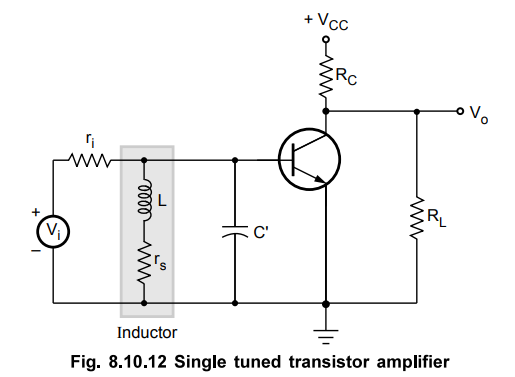
•
With these assumptions, the simplified equivalent circuit for a single timed amplifier
is as shown in Fig. 8.10.13.
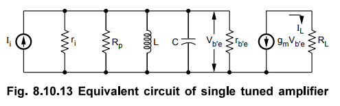
where C = C' + Cb,e + (1 + gm RL)
Cbc
(1
+ gm RL) Cbc : External capacitance used to tune the
circuit
(1
+ gm RL) Cbc The Miller capacitance
rs
: Represents the losses in coil
•
The series RL circuit in Fig. 8.10.12 is replaced by the equivalent RL circuit
in Fig. 8.10.13 assuming coil losses are low over the frequency band of
interest, i.e., the coil Q high.
Qc
≡ ωL / rs ... (8.10.16)
•
The conditions for equivalence are most easily established by equating the
admittances of the two circuits shown in Fig. 8.10.14.
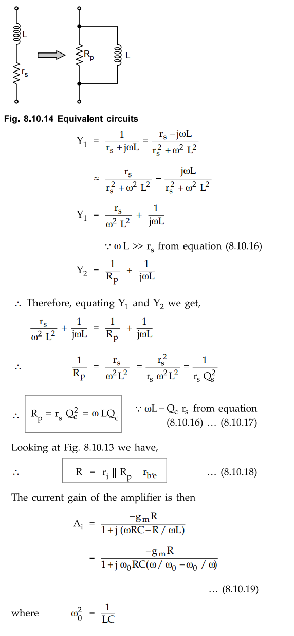
We
define the Q of the tuned circuit at the resonant frequenvy ω0 to be

•
The Fig. 8.10.15 shows the gain versus frequency plot for single tuned
amplifier. It shows the variation of the magnitude of the gain as a function of
frequency.
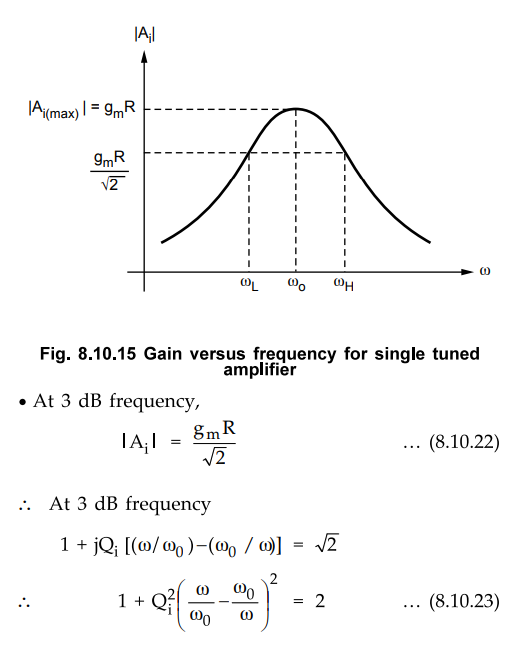
•
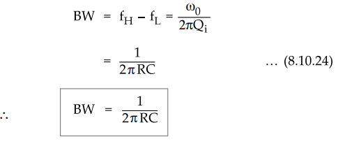
This equation is quadratic in ω2 and has two positive solutions, ωH
and ωL .After solving equation (8.10.23) we get 3 dB bandwidth as
given below.
Ex.
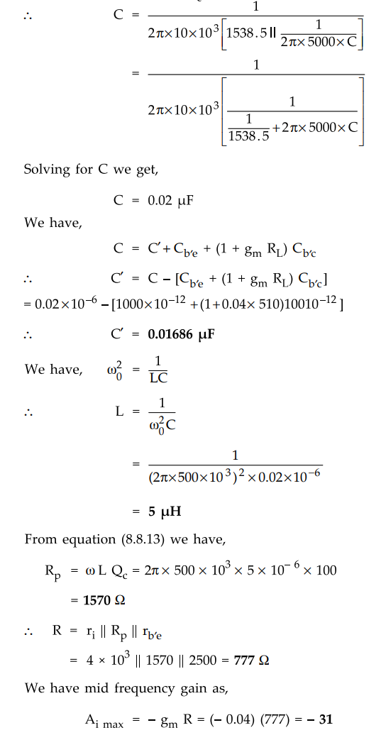
8.10.12 Design a single tuned amplifier for following specifications : 1.
Centre frequency = 500 kHz 2. Bandwidth = 10 kHz
Assume
transistor parameters : gm = 0.04 S, hfe = 100, Cbe = 1000 pF and Cb,c = 100
pF. The bias network and the input resistance are adjusted so that ri = 4 kΩ
and RL = 510Ω
Sol.
:
From equation (8.10.24) we have,
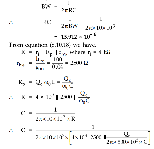
•
The typical range for Qc is 10 to 150. However, we have to assume Q„ such that
value of Cp should be positive. Let us assume Qc = 100.
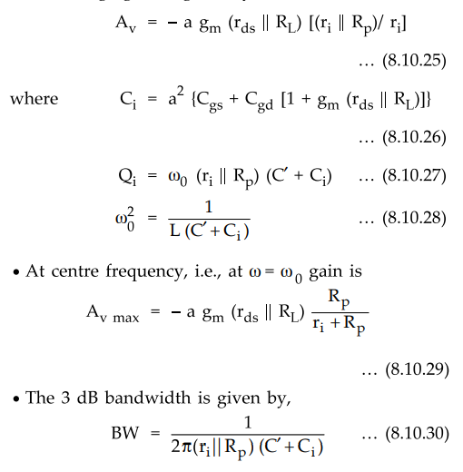
3. Single Tuned FET Amplifier
•
The Fig. 8.10.16 shows the single turned FET amplifier.
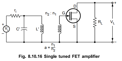
•
The wquivalent circuit for the given amplifier is as shown in the Fig. 8.10.17.

•
The voltage gain is given by,
Ex.
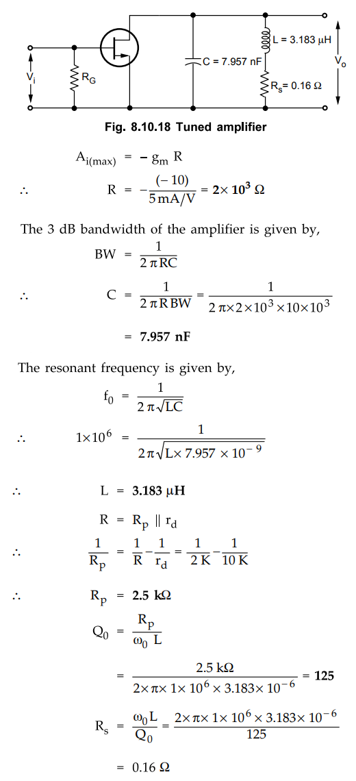
8.10.13 Design a tuned, amplifier using FET to have f0 = 1 MHz, 3 dB bandwidth
is 10 kHz and maximum gain is - 10 FET has gm = 5 mA/V, rd = 10 K.
AU
: May-06, Dec.-12, Marks 10
Sol.
:
The maximum gain of the amplifier is given by,
Electron Devices and Circuits: Unit IV: Multistage and Differential Amplifiers : Tag: : - Single Tuned Amplifiers
Related Topics
Related Subjects

Electron Devices and Circuits
EC3301 3rd Semester EEE Dept | 2021 Regulation | 3rd Semester EEE Dept 2021 Regulation