Electron Devices and Circuits: Unit IV: Multistage and Differential Amplifiers
Single Tuned Capacitive Coupled Amplifier
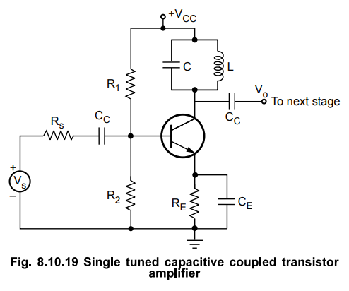
Single tuned multistage amplifier circuit uses one parallel tuned circuit as a load in each stage with tuned circuits in all stages tuned to the same frequency. Fig. 8.10.19 shows a typical single tuned amplifier in CE configuration.
4. Single Tuned Capacitive Coupled Amplifier
Single
tuned multistage amplifier circuit uses one parallel tuned circuit as a load in
each stage with tuned circuits in all stages tuned to the same frequency. Fig.
8.10.19 shows a typical single tuned amplifier in CE configuration.
•
As shown in Fig. 8.10.19 tuned circuit formed by L and C acts as collector load
and resonates at frequency of operation. Resistors Rj, and RE along with
capacitor CE provides self bias for the circuit.
•
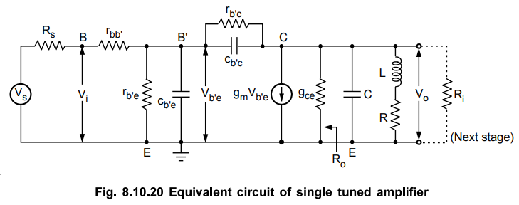
The Fig. 8.10.20 shows the equivalent circuit for single tuned amplifier using
hybrid n parameters.
•
As shown in the Fig. 8.10.20, Rj is the input resistance of the next stage and
RQ is the output resistance of the current generator gmVb'e. The reactances of
the bypass capacitor CE and the coupling capacitors Cc are negligibly small at
the operating frequency and hence these elements are neglected in the
equivalent circuit shown in the Fig. 8.10.20.
•
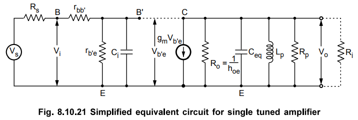
The equivalent circuit shown in Fig. 8.10.20 can be simplified by applying
Miller's theorem. Fig. 8.10.21 shows the simplified equivalent circuit for
single tuned amplifier.
•
Here C1 and Ceq represent input and output circuit
capacitances, respectively. They can be given as,
Ci
= Cbe + Cbc (1 – A)
where
A is the voltage gain of the amplifier. ... (8.9.31)
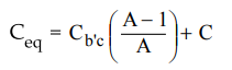
where
C is the tuned circuit capacitance. ...(8.10.32)
•
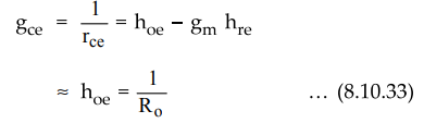
The gce is represented as the output resistance of current generator
gm Vbe
•
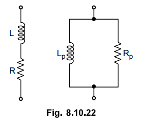
The series RL circuit is represented by its equivalent parallel circuit. The
conditions for equivalence are most easily established by equating the
admittances of the two circuits shown in Fig. 8.10.22.
•
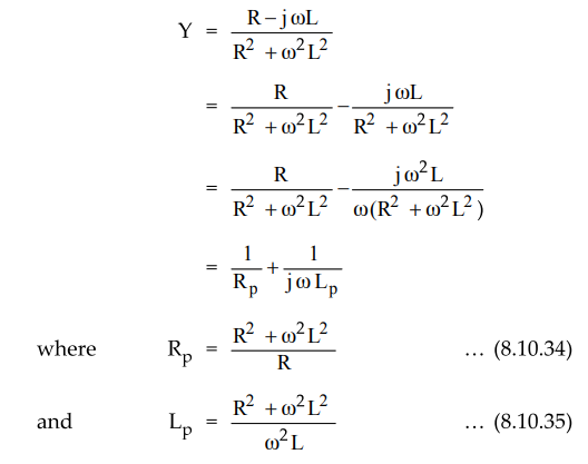
Admittance of the series combination of RL is given as,
Y
= 1 / R + j ωL
•
Multiplying numerator and denominator by R - jcoL we get,
Centre
frequency
•
The centre frequency or resonant frequency is given as,
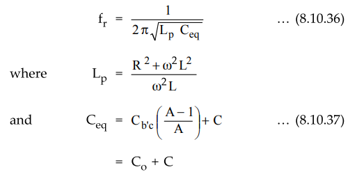
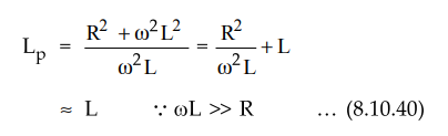
• Therefore Ceq is the summation of transistor output capacitance and the tuned circuit capacitance.
Quality
factor Q
•
The quality factor Q of the coil at resonance is given by,
Qr
= ωr L / R ... (8.10.38)
where
ωr is the centre frequency or resonant frequency.
•
This quality factor is also called unloaded Q. But in practice, transistor
output resistance and input resistance of next stage act as a load for the
tuned circuit. The quality factor including load is called as loaded Q and it
can be given as follows :
•
The Q of the coil is usually large so that m L >> R in the frequency
range of operation.
•
From equation (8.10.34) we have,
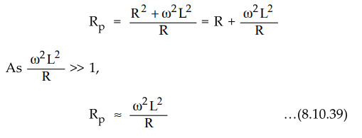
From
equation (8.10.39), we can express
Rp at resonance as,
Therefore,
Qr can be expressed interms of Rp as,
Qr
= Rp / ωr L … (8-10-42)
•
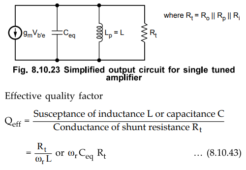
The effective quality factor including load can be calculated looking at the
simplified equivalent output circuit for single tuned amplifier.
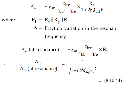
Voltage
gain (Av)
•
The voltage gain for single timed amplifier is given by,
3
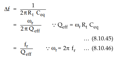
dB bandwidth
•
The 3 dB bandwidth of a single tuned amplifier is given by,
Ex.
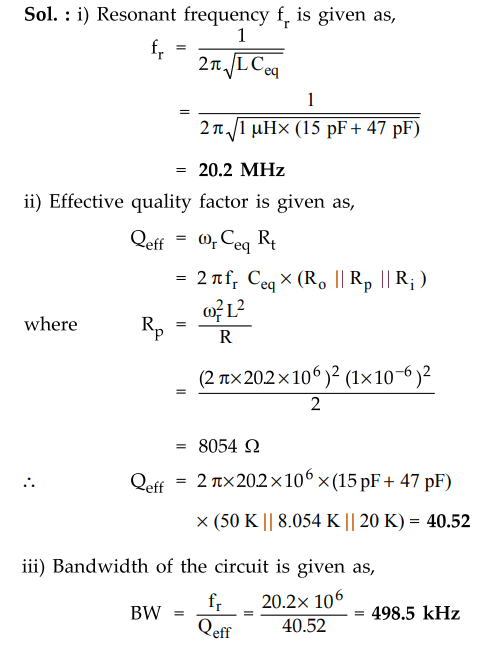
8.10.14 A single tuned RF amplifier uses a transistor with an output resistance
of 50 K, output capacitance of 15 pF and input resistance of next stage is 20 Ωl.
The tuned circuit consists of 47 pF capacitance in parallel with series combination
of 1 µH inductance and 2 Ω resistance. Calculate: i) Resonant frequency ii)
Effective quality factor iii) Bandwidth of the circuit.
Sol.
:
i) Resonant frequency f is given as,
Ex.
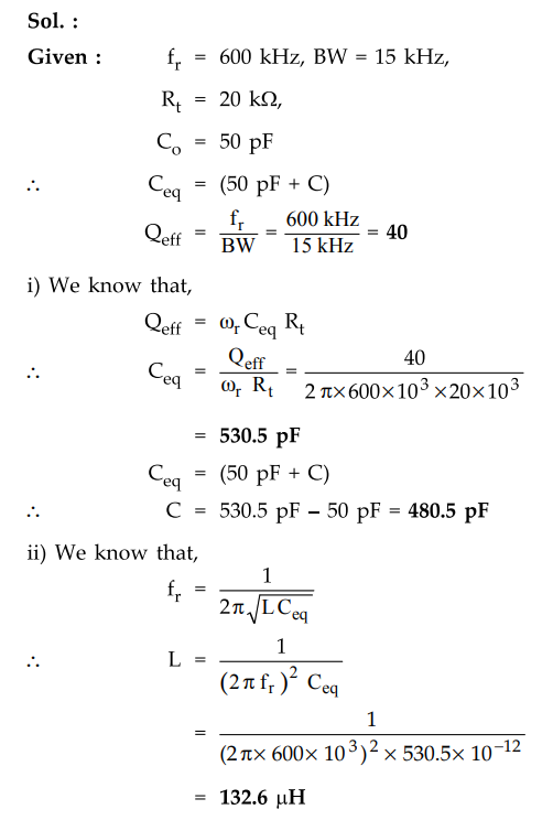
8.10.15 A single tuned transistor amplifier is used to amplify modulated RF
carrier of 600 kHz and bandwidth of 15 kHz. The circuit has a total output
resistance, Rt =20 kΩ and output capacitance CQ = 50 pF. Calculate values of
inductance and capacitance of the tuned circuit.
AU
: ECE : May-11, 12, Marks 4
Sol.
:
Review Questions
1. Derive the resonance frequency for the tank circuit.
2. Draw the ideal response and actual response of tuned amplifiers.
3. Draw the ideal tuned circuit and write the expression for
it's resonant frequency.
4. Define quality factor. Obtain the quality factor for a
parallel resonant circuit.
AU : ECE : Dec.-08, Marks 12
5. What is meant by unloaded and loaded Q of tank circuit ?
AU : ECE : May-03, Dec.-lO, Marks 2
6. What is the effect of Q on the resonance circuit ?
AU : ECE : Dec.-05, 07, Marks 2
7. Brief the relation between bandwidth and Q factor.
AU : ECE : May-07, Marks 2
8. With circuit diagram, a.c. equivalent circuit and frequency
response characteristics, explain the operation of a single tuned amplifier.
AU : ECE : Dec.-04, 09, 08, Marks 8
9. With equivalent circuit of single tuned amplifier derive the
gain as function of frequency. Derive the cut-off fsrequencies.
AU : ECE : May-06, Dec.-07, Marks 10
10. Explain single tuned voltage amplifier and discuss its
frequency response.
11. With neat sketch, explain the BJT differential amplifier
with active load and device for Ad, Ac and CMRR. How CMRR can be improved.
AU : Dec.-15, Marks 16
12. Discuss the working of single tuned amplifier.
AU : ECE : May-07, Dec.-l0, Marks 16
13. Derive the expression for gain and cut-off frequencies of
single tuned amplifier.
AU : ECE : Dec.-09, Marks 6
14. Draw the equivalent circuit of a single-tuned amplifier and
derive the expression for the gain as a function of frequency.
15. Draw the circuit diagram and the equivalent circuit of
capacitive coupled single tuned amplifier and explain its operation. Derive the
equation for voltage gain and the 3 dB bandwidth. Sketch also the frequency
response of the amplifier.
AU : ECE : May-11, 12, 13, Marks 12
16. Draw the frequency response of an ideal and a practical
tuned amplifier and discuss their characteristics.
AU : Dec.-05, 06, 07, 08, 09, 10, 11, 15, May-04, 06, 08, 09,
10, 11, 12
Electron Devices and Circuits: Unit IV: Multistage and Differential Amplifiers : Tag: : - Single Tuned Capacitive Coupled Amplifier
Related Topics
Related Subjects

Electron Devices and Circuits
EC3301 3rd Semester EEE Dept | 2021 Regulation | 3rd Semester EEE Dept 2021 Regulation