Electron Devices and Circuits: Unit III: (a) BJT Amplifiers
Small Signal Amplifier Performance In terms of h-parameters
Solved Example Problems | BJT Amplifiers
• The Fig. 6.4.1 shows basic amplifier circuit. It represents a transistor in any one of the three possible configurations.
Small Signal Amplifier Performance In terms of h-parameters
AU
: May-03, 05, 09, 15, 16, Dec.-05, 06, 14, 16
•
The Fig. 6.4.1 shows basic amplifier circuit. It represents a transistor in any
one of the three possible configurations.

•
Let us analyze hybrid model to find the current gain, the input resistance, the
voltage gain, and the output resistance.
Step
1 :
Draw the hybrid equivalent circuit
•
The Fig. 6.4.2 shows hybrid equivalent circuit for the amplifier circuit. It is
obtained by replacing the transistor by its h-parameter model.

Step
2 :
Obtain expression for current gain (AI )
•
For transistor amplifier, AI is defined as the ratio of output to
input currents. It is given by,
AI
= IL / I1 = - I2 / I1 ...(6.4.1)
•
Here IL and I2 are equal in magnitude but opposite in sign, i.e. IL=
- I2
•
From the circuit of Fig. 6.4.2 We have,
I2
= hf I1 + ho
V2 … (6.4.2)
•
Substituting V2 = - I2 RL in Equation (6.4.2)
we obtain,

Current
Gain (AIs ) :
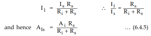
•
It is the current gain taking into account the source resistance, R s if the
model is driven by the current source instead of voltage source. It is given by

•
Looking at Fig. 6.4.3 (b) and using current divider equation we get

Step
3 :
Obtain expression for input resistance (Ri)
•
As shown in the Fig. 6.4.1, Ri is the input resistance looking into the
amplifier input terminals (1, 1'). It is given by,
Ri
= V1 / I1 ...
(6.4.6)
• From the input circuit of Fig. 6.4.2, we have

• Dividing numerator and denominator by RL we get
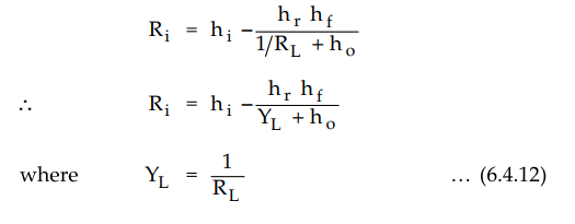
Important
Concept
From
this equation we can note that input impedance is a function of the load
impedance.
Step
4 :
Obtain expression for voltage gain (AV)
•
It is the ratio of output voltage V2 to the input voltage V1
It is given by
AV
= V2 / V1 … (6.4.1)
From
equation (6.4.9) we have,

Voltage
Gain (Avs) : It is voltage gain including the source. It is given
by,
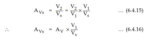
Looking
at Fig. 6.4.4 and applying potential divider theorem we can write,

•
Substituting value of V1 / Vs in equation (6.4.16) We get,

Step
5 :
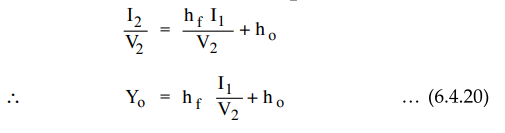
Obtain expression for output admittance (Yo)
•
It is the ratio of output current I2 to the output voltage V2.
It is given by,
Yo
= I2 / V2 with Vs = 0 ... (6.4.19)
•
From equation (6.4.2), we have,
I2
= hf I1 + ho V2 … (6.4.19)
•
Dividing above equation by V2 we get,
•
Applying KVL to the input loop of Fig. 6.4.2 we have,

•
Substituting value of from equation (6.4.22) in equation (6.4.20), we obtain,

Important
Concept
From
this equation we can note that output admittance is a function of the source
resistance.
Step
6 :
Obtain expression for power gain (AP)
•
It is the ratio of average power delivered to the load RL, to the
input power. Output power is given as
P2
= V2 IL = -V2I2 ... (6.4.24)
•
Since the input power is p = V1I1 the operating power
gain AP of the transistor is defined as

Relation
between AVs and AIs :
•
From equations (6.4.18) and equation (6.4.5) we have

•
Taking ratio of above two equations we get,

•
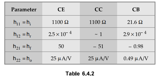
Table 6.4.1 summarizes small-signal analysis of a transistor amplifier

Important
Concept
The
above formulae is applicable to all transistor configuration. Only we have
added the appropriate subscript to h-parameters corresponding to the transistor
configuration in the expression of AI,Av,Ri Yo
•
Table 6.4.2 shows the typical values of h parameters for three different
configurations at normal room temperature and at quiescent operating point IEQ
= 7.3 mA
Ex.
6.4.1 Derive the expressions for AI, AV, Ri
and Ro for CE amplifier using h-parameter model.
AU
: Dec.-14, 16, May-15, Marks 16
Sol.
:
The Fig. 6.4.5 shows the CE amplifier and its h-parameter equivalent circuit.

•
Let us analyze hybrid model to find the current gain, the input resistance, the
voltage gain, and the output resistance.
Step
1 :
Obtain expression for current gain (AI )
Current
gain (AI) = IL /
Ib = Ic / Ib ... (1)
From
the circuit of Fig. 6.4.5 (b) we have,

Step
2 :
Obtain expression for input resistance (Ri)
Input
resistance (Ri) = Vb / Ib … (4)
From
the input circuit of Fig. 6.4.5 (b) we have,

Step
3 :
Obtain expression for voltage gain (AV )
Voltage
gain (AV ) =

Step
4 :
Obtain expression for output admittance (Yo)
Output
admittance (Yo) = Ic / Vc with Vs =
0 … (8)
From
equation (6.4.2), we have,
Ic
= hfe Ib + hoe Vc
Dividing
above equation by Vc we get,
Yo
= Ic / Vc = hfe Ib / Vc + hoe
From
Fig. 6.4.5 (b), with Vs = 0 we can write,

Substituting
value of Ib / Vc from equation (10) in equation (9), we
obtain,

Ex.
6.4.2 Consider a single stage CE amplifier with Rs = 1 K and RL = 1.2 k
Ω.
Calculate Ai, Ri, Av, AIs, power gain and Ro if hie = 1.1 K, hre = 2.5 × 10⁻⁴, hfe
= 50 and hoe = 25 µA/V.
Sol.

Ex.
6.4.3 Derive the expressions for current gain, voltage gain, input impedance
and output impedance for an emitter follower circuit.
AU
: ECE : May-03,05,09, Marks 10; Dec.-06
Sol.
:
The Fig. 6.4.6 shows the emitter follower (CC) amplifier circuit and its
h-parameter equivalent circuit.

Let
us analyze hybrid model to find the current gain, the input resistance, the
voltage gain and the output resistance.
Current
Gain (Ai) = IL / Ib = - Ie / Ib
... (1)
From
the circuit of Fig. 6.4.6 (b) we have,

From
the input circuit of Fig. 6.4.6 (b), we have,
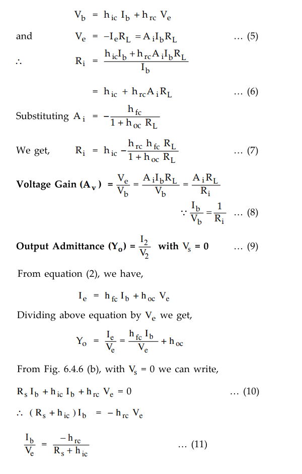
Substituting
value of Ib / Ve from equation (11) in equation (10), we
obtain,

Ex.
6.4.4 In the common collector in Fig. 6.4.7, the transistor parameters are hfc
= 1.2 K, hfc = -101, hrc = 1 and hoc = 25 µA/V. Calculate
the , Ri, AI = IL / Is, AD, AGS
= Vo / Vs , Ro for the circuit.

Sol.
:
Fig. 6.4.7 shows the h-parameters equivalent model for the given circuit,
a)
Current gain


Ex.
6.4.5 Derive the expressions for A^, Ay, Rt and Ro for CB amplifier using
h-parameter model.
AU
: ECE : Dec.-05, May-16, Marks 8
Sol.
:
The Fig. 6.4.8 shows the CB amplifier and its h-parameter equivalent circuit

From
the circuit of Fig. 6.4.8 (b) we have,
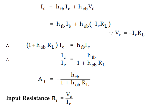
From
the input circuit of Fig. 6.4.8 (b) we have

Ex.
6.4.6 For the common base circuit in Fig. 6.4.9, the transistor parameters are
hib =22 Ω, hfc =- 0.98, hob = 0.49 µA/V, hrb = 2.9 × 10⁻⁴. Calculate the values
of the input resistance, output resistance, current gain and voltage gain for
the given circuit.
Sol.
:
Fig. 6.4.9 (a) shows the h-parameter equivalent model for the given circuit.

Review Question
1. Derive the expressions for the current gain, input impedance,
voltage gain and output admittance of a small signal CE transistor amplifier in
terms of the h-parameters.
Electron Devices and Circuits: Unit III: (a) BJT Amplifiers : Tag: : Solved Example Problems | BJT Amplifiers - Small Signal Amplifier Performance In terms of h-parameters
Related Topics
Related Subjects

Electron Devices and Circuits
EC3301 3rd Semester EEE Dept | 2021 Regulation | 3rd Semester EEE Dept 2021 Regulation