Linear Integrated Circuits: Unit V: Application ICs
Switching Regulators
Operating working principle, Functional Block Diagram, Types, Advantages, Disadvantages, Application
The operating principle of switching regulators is completely different than that of linear regulators. The switching regulators are also called as switched mode regulators.
Switching Regulators
Dec.-03,04,06,10,12,14,15,17,
May-06,07,08,09,10,11,15,16,17,18
The
operating principle of switching regulators is completely different than that
of linear regulators. The switching regulators are also called as switched mode
regulators. Such a switching regulator requires an external transistor and a
choke. The series pass transistor in such a regulator is used as a controlled
switch and is operated in cut-off region or saturation region. Hence the power
transmitted across such a transistor is in the form of discrete pulses rather
than a steady flow of current.
When
the transistor is operated in the cut-off region, there is no current and
dissipates no power. While when it is operated in the saturation region, a
negligible voltage drop appears across it and hence dissipates very small
power, providing maximum current to load. In any case, the power dissipated in
the transistor is very small. Almost the entire power gets transmitted to the
load. Hence the efficiency of the switching regulators is always very high.
Key
Point The pulse width modulation is the basic
principle of the switching regulators. The average value of repetitive pulse
waveform is proportional to the area under the waveform.
So
switching regulators use the fact that if duty cycle of the pulse waveform is
varied, the average value of the voltage also changes proportionally.
Key
Point The duty cycle of the pulse waveform is the
ratio of the on time ton to the period T of the pulse waveform.
Mathematically
it can be expressed as,
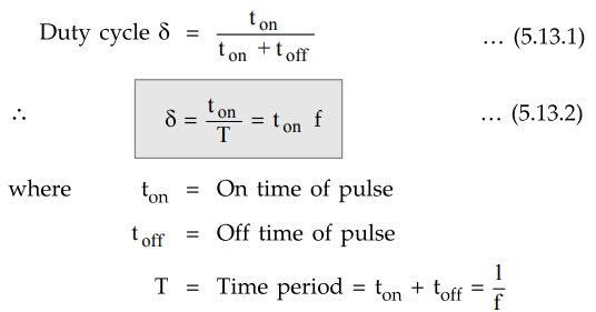
This
basic pulse width is shown in the Fig. 5.13.1.
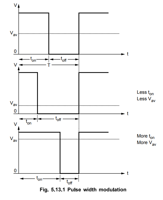
The
basic switching regulator consists of four major components :
a)
Voltage source Vin
b)
Switching transistor
c)
Pulse generator, Vpulse
d)
Filter F1
These
blocks are connected together as shown in the Fig. 5.12.2, to obtain the
switching regulator.
A
voltage source Vin is a d.c. supply which is a battery, unregulated
or regulated voltage.
It
has to satisfy the requirements as :
i)
It has to supply required power and the losses associated with the regulator.
ii)
It must be high to satisfy the minimum requirements of the regulator.
iii)
It must be large to supply sufficient dynamic range of line and load changes.
The
switch is generally a transistor. The pulse generator output makes it on and
off. The pulse generator produces a required pulse waveform. The most effective
range of pulse waveform frequency is 20 kHz. The typical operating frequency
range is 10 to 50 kHz. The filter F1 may be RC, RL or RLC. Most
commonly used filter is RLC. It converts the pulse waveforms obtained from the
switch into a d.c. output voltage.
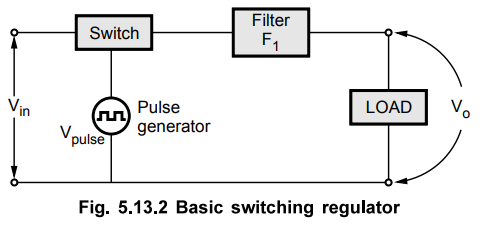
1. Block Diagram of SMPS
The
Fig. 5.13.3 shows the functional block diagram of basic switching voltage
regulator, which uses transistor Q1 as a switch.
The
part R2/R1 + R2 of the output is fedback to
the inverting input of error amplifier. It is compared with the reference
voltage. The difference is amplified and given to the comparator inverting
terminal.
The
oscillator generates a triangular waveform at a fixed frequency. It is applied
to the non-inverting terminal of the comparator. The output of the comparator
is high when the triangular voltage waveform is above the level of the error
amplifier output. Due to this the transistor Q1 remains in cut-off
state. Thus the output of the comparator is nothing but a required pulse
waveform.
The
period of this pulse waveform is same as that of oscillator output say T. The
duty cycle is denoted as 5 = ton/T or ton f as mentioned earlier.
This duty cycle is controlled by the difference between the feedback voltage
and the reference voltage.
When
Q1 is on in saturation state, VCE(sat) for Q1
is zero. Hence entire input voltage appears at point A. Thus the current flows
through inductor L1.
When
Q1 is off, L1 still continue to supply current through
itself to the load. The diode D1 provides the return path for the
current.
The
capacitor C1 acts to smooth out the voltage and the voltage at the
output is almost d.c. in nature. The output voltage Vo of the
switching regulator is a function of duty cycle and the input voltage V^.
Mathematically it is expressed as,
Vo
= (ton / T) Vin = δ Vin … (5.13.3)
Thus
when T is constant, output is proportional to ton. This method is called Pulse
Width Modulation (PWM). When ton is constant, the output is inversely
proportional to the period T i.e. proportional to frequency of the pulse waveform.
This method is called frequency modulation.
Key
Point The PWM technique is commonly used though it is
more complex as it is most suitable for the high current applications.
A
high switching frequency allows small values of L1 and C1
and thus reduces size, cost and weight. It also reduces the ripple at the
output. But the efficiency decreases and electrical noise increases. On the
other hand, low switching frequency improve efficiency and reduce noise but
require large filtering components. As a result of this, the range of operating
frequency to get maximum efficiency, is 10 to 50 kHz.
2. Types of Switching Regulators
The
term switched mode regulator is used to describe a circuit which takes d.c.
input (unregulated) and provides a single d.c. output of the same or opposite
polarity, and of a lower or higher voltage. The switched mode regulators use an
inductor and there is no input to output isolation.
The
term switched mode converter is used to describe a circuit which takes d.c.
input (unregulated) and provides single or multiple d.c. outputs, again of same
or opposite polarity and of a lower or higher voltage. Converters use
transformer and may provide input to output isolation.
There
are three basic configurations of the switching regulators.
1.
Step down or Buck switching regulator
2.
Step up or Boost switching regulator.
3.
Inverting type switching regulator.
Let
us discuss the operation of three types of switching regulators.
3. Step Down Switching Regulator
The
Fig. 5.13.4 shows the basic circuit of step down switching regulator, which is
also called buck type switching regulator.
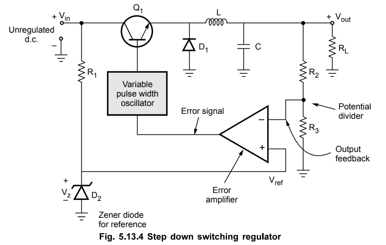
It uses an inductor L and series transistor Q1
which acts as a switch. The reference for error amplifier is provided by zener
voltage Vz. The output is fed back to error amplifier through
potential divider. The pulse width oscillator controls the operation of Q1
as on or off, depending on the load requirements.
Consider
an equivalent circuit of the regulator as shown in the Fig. 5.13.4 (a). In this
circuit, Q1 is shown as a switch as it does the function of a
switch.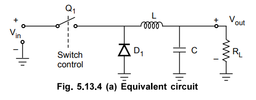
The transistor Q1 is used for switching the input voltage for the required period of time, which is dependent on load current requirement. The L-C filter averages the switched voltage.
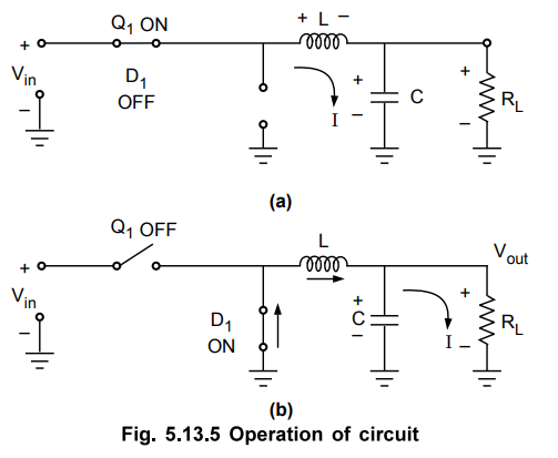
Operation
:
When Q1 is ON, the capacitor charges through it and when Q1
is OFF, the capacitor discharges through the load resistance, as shown in the
Fig. 5.13.5 (a) and (b).
The
variable pulse width oscillator controls ON/OFF periods of Q1 When
ON time is more compared to OFF time, the capacitor charges more, increasing
the output voltage. On the other hand, when OFF time is more than ON time for Q1
the capacitor discharges more, reducing output voltage. Thus adjusting
the duty cycle δ = (ton / ton + toff) of Q1
output voltage can be regulated.
If
the output voltage increases, the voltage across R3 increases. The
reference Vz is fixed. Thus error at the input of error amplifier
decreases. The output of error amplifier controls the output of variable pulse
width oscillator. It produces pulse of smaller width which reduces ton for Q1
This makes the capacitor C to discharge more, to offset any attempt of increase
in output voltage.
Thus
output voltage is maintained constant by controlling duty cycle of Q1.
The
output voltage is given by,
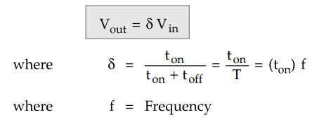
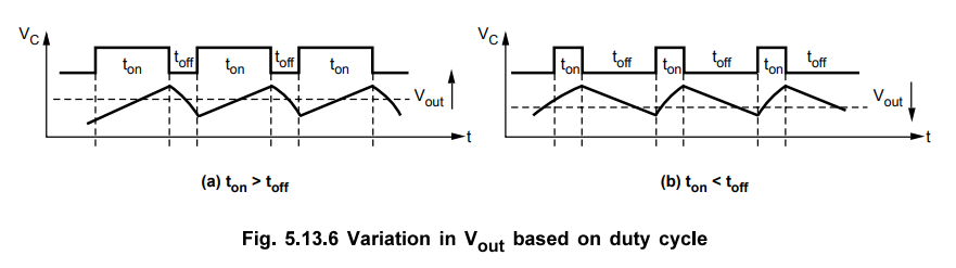
The
Fig. 5.13.6 shows the waveform of capacitor voltages for ton > toff
and ton < toff.
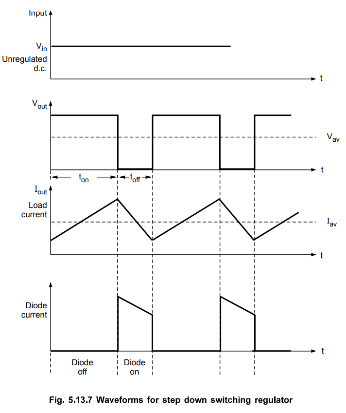
The
waveforms for step down switching regulator are shown in the Fig. 5.13.7.
a.
Advantages
The
advantages of buck regulator are,
1.
Higher efficiency.
2.
Simple to design.
3.
Low ripple content.
4.
Small output filter.
5.
Low switch stress.
6.
Large tolerance of line voltage regulation.
7.
Low cost, size and weight.
b.
Disadvantages
The
disadvantages of buck regulator are,
1.
Single output.
2.
No isolation between input and output
3.
High input ripple current.
4.
The input voltage must be always slightly greater than output (by 1 or 2 V).
5.
Slow transient response compared to linear regulator.
6.
Due to finite reverse recovery time of commutating diode, the instantaneous
short circuit occurs across the source, due to which active switches may fail.
4. Step Up Switching Regulator
The
Fig. 5.13.8 shows the basic circuit of step up switching regulator which is
also called boost type switching regulator.
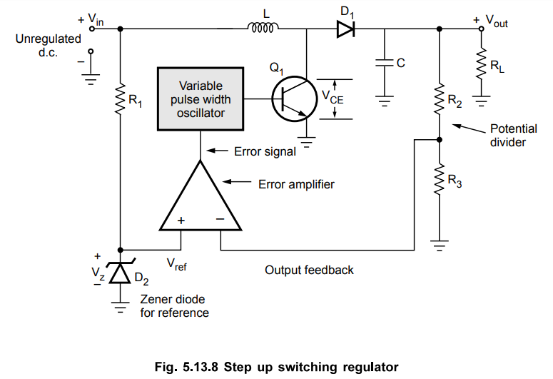
The
basic elements used in this type are identical to those used in step down type
but their arrangement is different.
The
transistor Q1 works as an on/off switch. When Q1 is
driven into saturation, VCE is very very small and it acts as short
circuit. When Q1 is driven into cut-off, it is off and it acts as an
open circuit. Let us study these two cases in detail.
Case
1 :
Let Q1 is ON i.e. driven to saturation.
When
Q1 is ON, VCE is denoted as VCE(sat) and the voltage
across L suddenly becomes [Vin - VCE(sat)] as shown in
the Fig. 5.13.9 (a). This expands the magnetic field around the inductor very
quickly. This voltage across L can be obtained by applying KVL to Vin,
L, Q1 and Vin closed path.
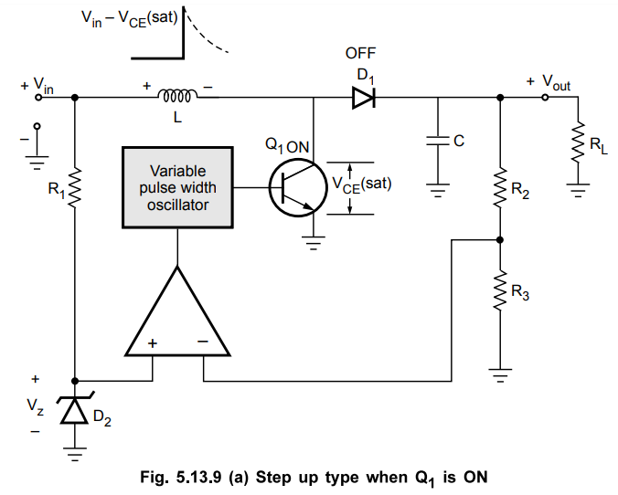
During
the ON time (ton) of Q1, the voltage across the inductor starts decreasing
exponentially from its initial maximum value [Vin – VCE(sat)]
Key
Point The longer the on time of Qlf the smaller will
be the voltage across L.
Case
2 :
Let Q1 is switched OFF i.e. cut-off region. When Q1 is
OFF, the magnetic field of the inductor L collapses and its polarity gets
reversed. This is because an inductor current can not change instantly. Thus
value of VL attained after exponential decrease when Q1
is ON, now gets reversed as shown in the Fig. 5.13.9 (b). Due to reversal of
polairty, it gets added to Vin.
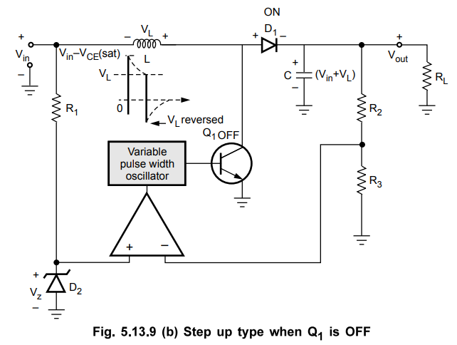
Trace
the path Vin, L, D1, C and Vin. The diode D1
is forward biased due to reversed VL and capacitor C now charges to
Vin + VL. The output voltage is voltage across capacitor
C which is Vin + VL, which is more than Vin. Thus it acts
as step up type regulator.
It
can be seen that how much VL should be added to i.e. by how much
output should be stepped up can be controlled by ON period of Q1.
The shorter the ON period of Q1 the greater is VL as it
will not decrease much and the greater voltage will get added to V^, increasing
the output voltage. The longer the ON time of Q1 the smaller is the
inductor voltage VL and less voltage will get added to V^,
decreasing the output voltage.
When
output voltage tries to decrease due to increase in load current or decrease in
itself then ON time of Q1 gets reduced, thus increases compensating
for the decrease in it.
When
output voltage tries to increase, then ON time of Q1 gets increased.
This reduces the flyback voltage i.e. voltage across the inductor. Thus the
less voltage gets added to Vin, reducing it s value. This
compensates for the attempted increase in the output voltage.
Expression
for the output voltage
The
output voltage is given by,
Vout
= Vin / 1 – δ
where
δ = ton / T
The
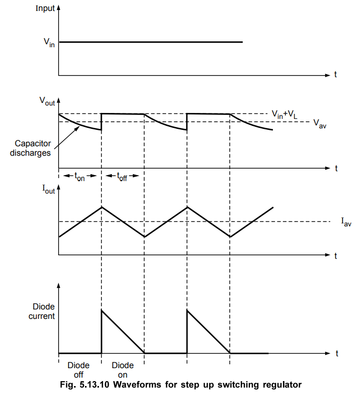
waveforms for step up switching regulator are shown in the Fig. 5.13.10.
a.
Advantages
The
advantages of boost regulator are :
1.
The output voltage is higher than input voltage.
2.
The efficiency is high, greater than 90 %.
3.
Low input ripple current.
4.
Simple to design.
b.
Disadvantages
The
disadvantages of boost regulator are :
1.
It provides single output.
2.
The duty cycle is limited to 50 % to avoid the continuous current mode. If
regulator enters the continuous current mode, it stops regulating the output.
Thus for a minimum input voltage range, maximum duty cycle is limited.
3.
Due to restricted duty cycle, the peak collector current is very high. This
limits its output power rating.
4.
No isolation between input and output. Any surge or transient in input can
reach to output directly.
5. Voltage Inverter Type Switching Regulator (Buck-Boost)
This
type of switching regulator produces an output voltage having polarity opposite
to that of the input voltage. This is also called buck boost type switching
regulator. The Fig. 5.13.11 shows voltage inverter type switching regulator.
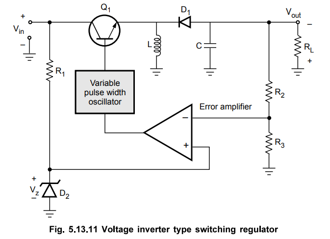
The
elements are again identical to buck and boost type regulators but their
connections are different. The basic action remains same. Any change in output
produces error which gets amplified by op-amp error amplifier. This controls the
on/off periods of Q1 to regulate the output, through variable pulse
width oscillator.
Let
us analyse two cases.
Case
1 :
Let Q1 is switched ON.
The
Q1 goes into saturation and the voltage across it drops to VCE(sat)
which is about 0.3 V. Due to this voltage across inductor suddenly rises to [Vin
- VCE(sat)] and magnetic field around it suddenly expands. Due
to connection of diode D1 in this situation, it is reverse biased.
This is shown in the Fig. 5.13.12 (a).

The
inductor voltage starts exponentially decresing from the intial value [Vin
- VCE(sat)]
Case
2 :
Let Q1 is OFF.
Now
if Q1 is turned OFF, the magnetic field across L gets collapsed. But
inductor current cannot change instantaneously. Thus voltage across inductor VL
reverses its polarity as shown in the Fig. 5.13.12 (b).
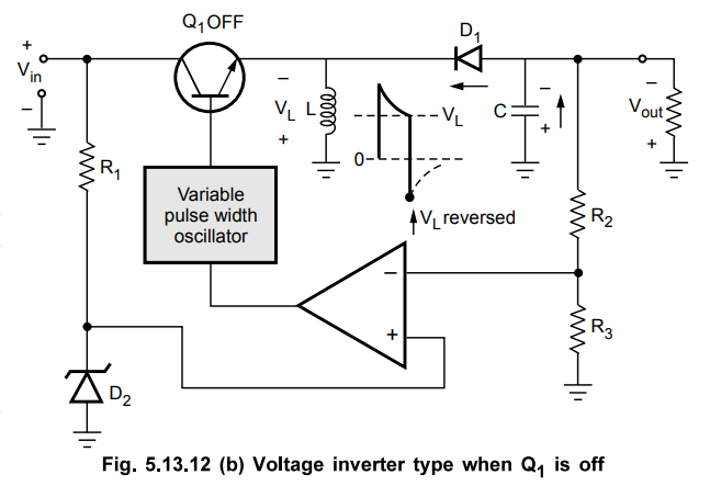
Due to reversed VL, the diode D1 is now forward biased. The capacitor charges through D1 producing output voltage of opposite polarity to that of Vin. Hence the regulator is called voltage inverter type.
The repetitive on-off action of Q1 produces a repetitive charging and discharging of the capacitor C which is smoothed by the LC filter action. The less period Q1 is ON, higher is the output voltage, the greater time Q1 is ON, smaller is the output voltage.
The
advantages and disadvantages of this type are same as that of step up type
regulator.
6. Application of SMPS
Depending
upon the requirements such as low cost, isolation, multiple outputs, step up
output, inverted output, step down output, output current, variable load
current etc, various types of SMPS are used in the following variety of
applications,
1.
Adjustable high voltage constant current sources.
2.
Battery powered systems.
4.
Personal computers.
5.
Printers
6.
Video games.
7.
Motor and industrial control systems.
8.
Automotive applications.
a.
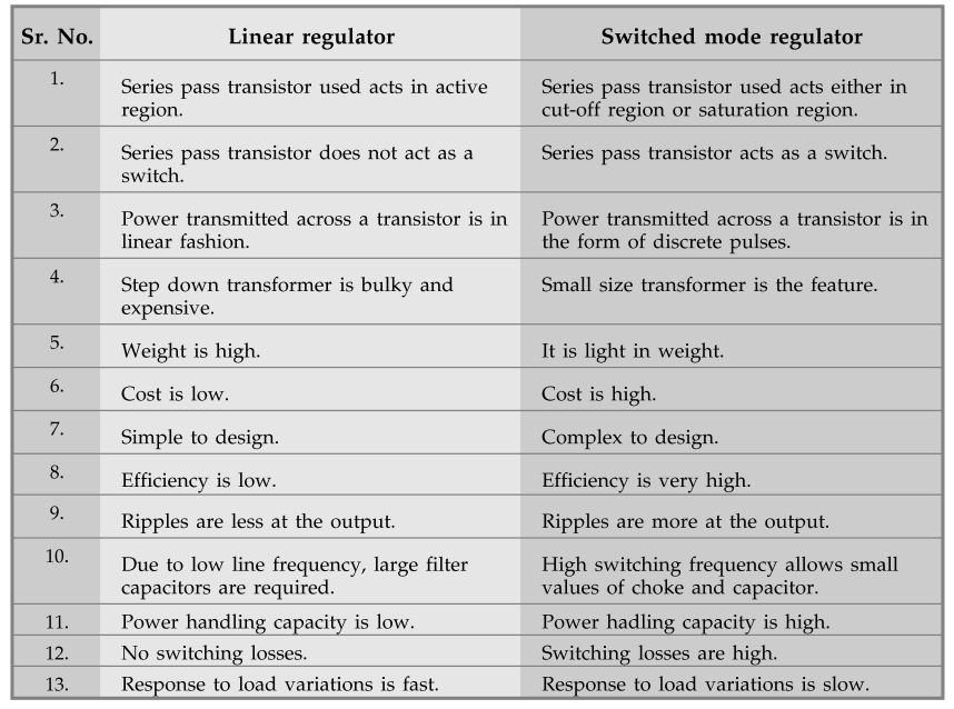
Comparison of SMPS Linear Regulators
Review Questions
1. State differences between linear mode and switched mode power
supply. Draw the complete block diagram of switching regulator and explain its
operation.
10, Dec.-14, Marks 8
2. Explain the operation of switching regulator. Give its
advantages.
Dec.-10, 17, May-16, 17, Marks 16
3. Write a note on
switching regulator.
Dec.-12, May-18, Marks
8
4. What is the
principle of switch-mode power supplies? Discuss its advantages and
disadvantages.
May-15, Marks 8
5. Compare linear
regulator with switched mode regulator.
6. With neat diagram
explain the working of step down switching regulator.
May-06, 11, Dec.-12,
14, Marks 16
7. Briefly explain the working principle of step up switch mode power supply with necessary circuit diagram and waveforms.
8. Explain the working of voltage inverter type switching
regulator.
Linear Integrated Circuits: Unit V: Application ICs : Tag: : Operating working principle, Functional Block Diagram, Types, Advantages, Disadvantages, Application - Switching Regulators
Related Topics
Related Subjects

Linear Integrated Circuits
EE3402 Lic Operational Amplifiers 4th Semester EEE Dept | 2021 Regulation | 4th Semester EEE Dept 2021 Regulation