Linear Integrated Circuits: Unit V: Application ICs
Three Terminal Adjustable Regulators: LM 317
Schematic diagram, Functional Block Diagram, Applications, Solved Example Problems
Besides fixed voltage regulators, IC voltage regulators are available which allow the adjustment of the output voltage. The output voltage can be adjusted from 1.2 V to as high as 57 V with the help of such regulators.
Three Terminal Adjustable Regulators : LM 317
Besides
fixed voltage regulators, IC voltage regulators are available which allow the
adjustment of the output voltage. The output voltage can be adjusted from 1.2 V
to as high as 57 V with the help of such regulators. In such regulator ICs the
common terminal plays the role of control input and hence called as ADJUSTMENT
(ADJ) terminal. The LM317 series is the most commonly used three terminal
adjustable regulators. These devices are available in a variety of packages
which can be easily mounted and handled. The power rating of such regulators is
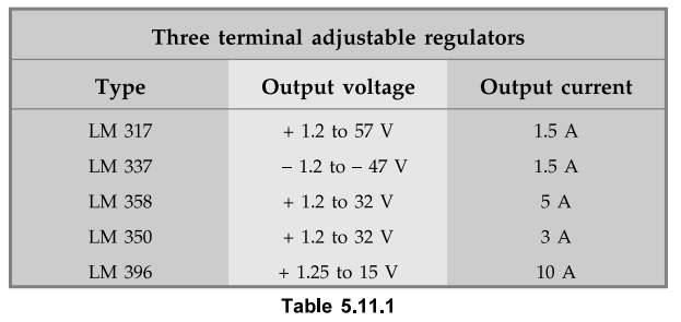
1.5 A. The maximum input voltage of LM317 is 40 V. The Table 5.11.1 shows the
various types of adjustable regulators and the corresponding output voltage
range and maximum output current rating.
Adjustable
voltage regulators have the following advantages over fixed voltage regulators,
1)
Improved line and load regulation by a factor of 10 or more.
2)
Because of improved overload protection, greater load current can be drawn over
the given operating temperature range.
3)
Improved reliability for the power supply using these regulators.
Thus,
adjustable voltage regulators have become more popular because of their
versatility, performance and reliability. The LM 317 is the most widely used adjustable
voltage regulator series.
1. Connection Diagram of LM 317 Regulator
The
typical connection diagram of LM 317 regulator is shown in the Fig. 5.11.1.
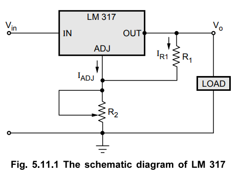
The
LM 317 requires only two external resistances R1 and R2,
to set the required output voltage. Internally it develops a reference voltage
of 1.25 V between OUT and ADJ terminals, which is denoted as VREF.
This voltage is impressed across the resistance
R1.
So for constant VREF and R1 current IR1 is
also constant. So resistance R1 which sets the current IR1
is called current set resistor or program resistor.
The
current IADJ flows out from the ADJ terminal and is quiescent
current IQ voltage regulators. This current, along with IR1,
flow through the resistance R2.
The design of LM 317 is such that Fi3- 5-11-1 The schematic diagram of LM 317
the current IADJ is very small and remains constant with line and
load changes. The maximum value of IADJ is 100 µA which is very
small.
By
KVL, we can write,
The
current IADJ is very small and hence the drop IADJ R2
is also very small and can be neglected.
Vo
= 1.25[ 1 + R2 / R1]
… (5.10.4)
Thus
the output voltage is a function of R1 and R2. Keeping R1
fixed and varying R2, the output voltage can be adjusted. The program
resistor R1 is generally 240 Ω.
Generally
no capacitors are required. But if LM 317 is located far from the power supply
filter then the capacitors C1 and C2 are required. The
input capacitor C1 is generally 0.1 µF disc or 1 µF tantalum while the output
capacitor C2 is in the range of 1 to 1000 µF. To get high ripple
rejection, the capacitor C3 is used. To avoid the discharging of the
capacitors through low current points into the regulator, the protecting diodes
are used. The Fig. 5.11.2 shows the functional diagram of LM 317 alongwith the
capacitors and the protecting diodes.
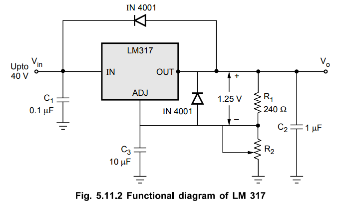
Key
Point The diodes are necessary if output voltage is higher
than 25 V.
Applications
1.
Various electronic circuits. 2. Medical and fitness applications
3.
Printers 4. Various appliances 5. T.V. sets and set top boxes
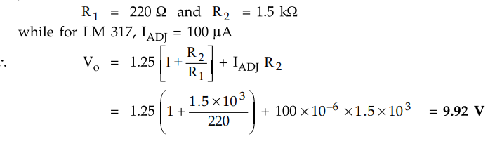
Example
5.11.1 Determine the regulated output voltage for
the LM 317 voltage regulator shown in the Fig. 5.11.3.
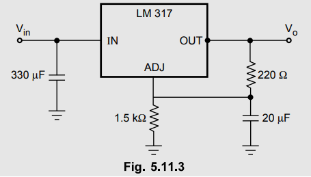
Solution
:
The resistances used are,
Example
5.11.2 Find the range in which output voltage can be varied
with the help of LM 317 regulator using R1 = 820 Ω and R2
as 10 k Ω potentiometer.
Solution
:
For LM 317, the current IADJ = 100 µA
When
R2 is minimum i.e. R2 = 0 then,
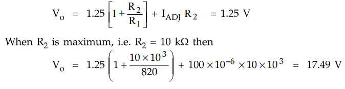
Thus
the output voltage can be varied in the range 1.25 V to 17.49 V
Review Questions
1. Draw and explain the
functional block diagram of the LM 317 three terminal adjustable regulator.
Dec,-03, Marks 12
2. What do you mean by
variable voltage regulator ? List its applications.
May-07, Dec.-16, Marks
8
Linear Integrated Circuits: Unit V: Application ICs : Tag: : Schematic diagram, Functional Block Diagram, Applications, Solved Example Problems - Three Terminal Adjustable Regulators: LM 317
Related Topics
Related Subjects

Linear Integrated Circuits
EE3402 Lic Operational Amplifiers 4th Semester EEE Dept | 2021 Regulation | 4th Semester EEE Dept 2021 Regulation