Linear Integrated Circuits: Unit V: Application ICs
Three Terminal Fixed Voltage Regulators
Features, Functional Block Diagram, Performance parameters, Applications, Solved Example Problems
As the name suggests, three terminal voltage regulators have three terminals namely input which is unregulated (Vin), regulated output (Vo) and common or a ground terminal. These regulators do not require any feedback connections. The Fig. 5.9.1 shows the basic three terminal voltage regulator.
Three Terminal Fixed Voltage Regulators
May-04,17.
Dec.-07,10,16
As
the name suggests, three terminal voltage regulators have three terminals
namely input which is unregulated (Vin), regulated output (Vo)
and common or a ground terminal. These regulators do not require any feedback
connections. The Fig. 5.9.1 shows the basic three terminal voltage regulator.
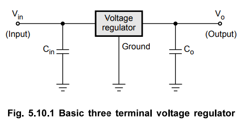
The
capacitor Cin is required if regulator is located at appreciable
distance, more than 5 cm from a power supply filter. The output capacitor Co
may not be needed but if used it improves the transient response of the
regulator i.e. regulator response to the transient changes in the load. This
capacitor also reduces the noise present at the output. The difference between
and Vo (Vin - Vo) is called as dropout voltage and it
must be typically 2.0 V even during the low point on the input ripple voltage,
for the proper functioning of the regulator.
1. Block Diagram of Basic Three Terminal IC Regulator
The
Fig. 5.10.2 shows the functioal block diagram of basic three terminal IC
regulator.
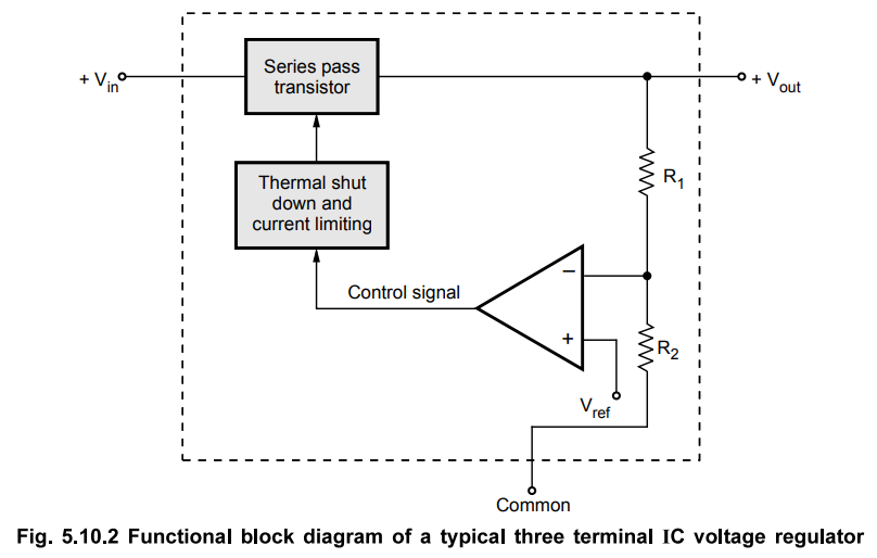
This
is basically a series voltage regulator circuit. A part of output voltage is
taken with the help of potential divider formed by R1 and R2.
This is compared with reference voltage, Vref internally generated with the
help of zener diode. After comparison, a control signal is generated which is
applied through protective circuit to the series pass transistor working as
control element. This element works as a variable resistance. The control
signal adjusts the control element in such a way that output voltage remains
constant.
Thermal
shutdown means that the chip will automatically turn itself off if the internal
temperature exceeds, typically, 175 °C. The current limiting circuit will
protect the chip from excessive load current. Because of the thermal shutdown
and current limiting, the IC voltage regulator chip is almost indestructible.
2. Datasheet Specifications of IC Linear Regulators
A
number of performance parameters are generally specified for the IC voltage
regulators by the manufacturers. These are as follows :
i)
Line regulation : It is defined as the change in the
output voltage for a given change in the input voltage. It is expressed as a
percentage of output voltage or in millivolts.
ii)
Load regulation : As defined earlier, it is the change in
output voltage over a given range of load currents i.e. from full load to no
load. It is usually expressed in millivolts or as a percentage of output
voltage.
iii)
Ripple rejection : It indicates regulator's ability to
reject ripple voltage present in the input. It is defined as the ratio of the
r.m.s. input ripple voltage to the r.m.s. output ripple voltage. It is
expressed in decibels (dB).
iv)
Dropout voltage : It is the minimum voltage that must
exist between input and output terminals. As mentioned earlier, it is the difference
between input voltage and output voltage Vo. For most of the regulators it is 2
to 3 V.
v)
Output resistance (Ro) : It is the rate of
change of output voltage with respect to the output current. It should be as
small as possible.
vi)
Maximum input voltage (Vin max) : This is the
maximum input voltage that can be applied to the regulator safely.
vii)
Maximum power dissipation (PDmax) :
This is the maximum power which regulator can dissipate without damage. The
actual power dissipated is approximately equal to the voltage drop between the
input and the output terminals multiplied by the current through the regulator.
For many regulators it is internally limited.
viii)
Quiescent current (IQ) : It is also called as
standby current. This is the supply current drawn by the regulator without any
load. It can also be defined as the current that must flow from the ground
terminal of the regulator to operate satisfactorily.
ix)
Rated output current (Io) : It is the maximum value
of the output current above which current limiting occurs.
x)
Output noise voltage : It indicates the tendency of the
output voltage to fluctuate above its prescribed d.c. value, over a specified
frequency range.
xi)
Maximum operating junction temperature : It is the maximum
value of junction temperature above which thermal shutdown occurs.
Out
of these parameters maximum input voltage, maximum power dissipation, maximum
operating junction temperature etc. are called as absolute maximum ratings of
IC regulator, while other ratings are called as electrical characteristics of
IC regulator.
3. LM 78XX and 79XX Three Terminal IC Voltage Regulators
The
popular IC series of three terminal regulators is pA 78XX and µA 79XX. The
series µA 78XX is the series of three terminal positive voltage regulators
while µA 79XX is the series of three terminal negative voltage regulators. The
last two digits denoted as XX, indicate the output voltage rating of the IC.
Such
series is available with seven voltage options as indicated in Table 5.10.1.
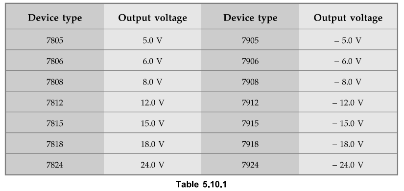
The
79XX series voltage regulators are available with same seven options as 78XX
series, as indicated in Table 5.10.1. In addition, two extra voltages -2 V and
-5.2 V are also available with ICs 7902 and 7905.2 respectively.
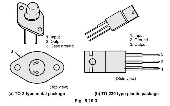
These
ICs are provided with adequate heat sinking and can deliver output currents
more than 1 A. These ICs do not require external components. These are provided
with internal thermal protection, overload and short circuit protection.
The
two series are available in various versions like low power and high power
versions. The low power versions are available in plastic or metal packages,
like small signal transistors. The higher power versions are packaged in TO-3
type metal cans or in TO-220 type moulded plastic packages like power
transistors.
These
are shown in the Fig. 5.10.3 (a) and (b).
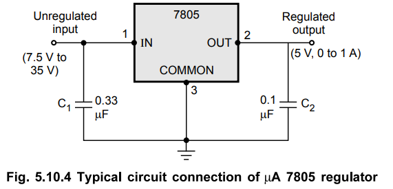
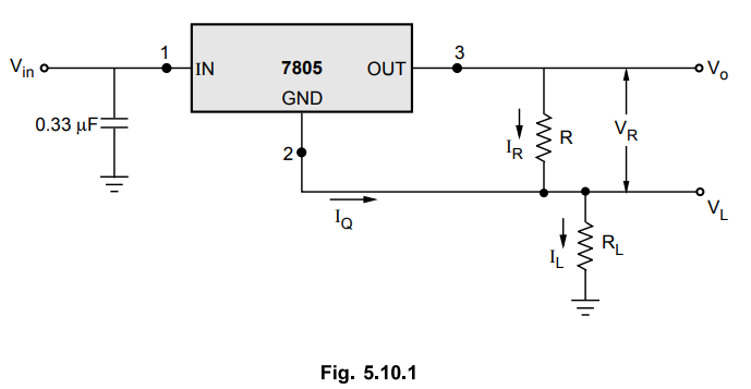
4. Typical Connection of IC 7805 Regulator
The
Fig. 5.10.4 shows the typical connection of IC pA 7805 regulator. The maximum
input voltage which can be applied to IC 7805 is 35 V. The maximum dropout
voltage is 2.5 V. The output of 7805 regulator is 5 V fixed. Hence minimum
input voltage required is 5 + 2.5 = 7.5. So input range of IC 7805 regulator is
7.5 V to 35 V to get fixed 5 V as regulated output. This is indicated in the
Fig. 5.10.4.
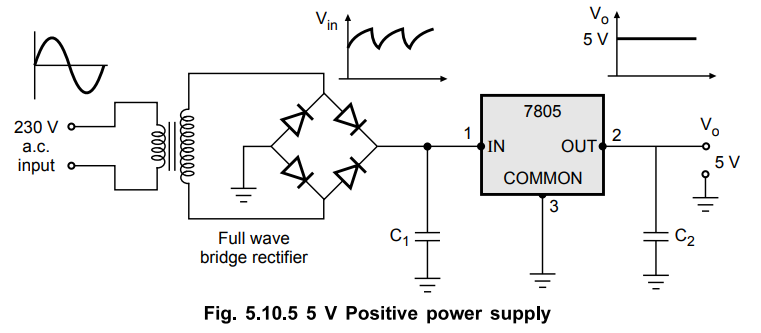
5. Positive 5 V Power Supply using IC 7805
A
5 V output voltage supply system using full wave bridge rectifier, capacitor
filter and IC regulator 7805 is shown in the Fig. 5.10.5. The a.c. line voltage
is 230 V which is stepped down to 15 V using a transformer. A full wave
rectifier alongwith the capacitor voltage provides the unregulated voltage
input to IC 7805 regulator. This input contains a.c. ripple of few volts. The
IC 7805 regulator provides the regulated output of 5 V.
6. Adjustable Regulator using 78XX Series
Though
IC 78XX series regulators have fixed value of the regulated output voltage, by
connecting two resistances externally, an adjustable output voltage can be
obtained.
The
typical connection of 78XX IC regulator to obtain variable output voltage is
shown in the Fig. 5.10.6.
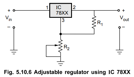
Vout
= Vreg [1+ R2 / R1]
where
Vreg = Regulated fixed voltage of IC
By
varying R2, variable output voltage can be obtained.
7. Applications of IC 78XX and 79XX
These
ICs are regulator ICs and are basically used to provide constant d.c. voltages
to various components in complex electronic circuits.
The
IC 7805 is typically used to provide constant 5 V supply to the digital
circuits.
The
IC 7812 and 7912 are used to provide dual supply of ± 12 V to operational
amplifiers used in the electronic circuits.
Example
5.10.1 Calculate the output voltage of the adjustable
regulator shown in the Fig. 5.10.7.
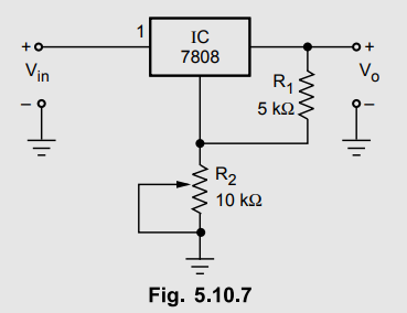
If
R2 is varied from 1 kΩ to 10 kΩ find the range of output voltage.
Solution
:
R1 = 5 kΩ, R2 = 10 kΩ
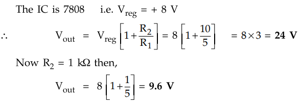
Thus
the Vout can be varied from 9.6 V to 24 V, by varying R2
from 1 kΩ to 10 kΩ .
8. Boosting Regulator Output Current
For
limiting the cost and size, if output current as high as 10 A is required then
it is convenient to boost a regulator output current, which is of less
capacity, with the help of external circuit.
The
three terminal regulators can be boosted by connecting an external pass
transistor in parallel with the regulator itself. Due to this the maximum
output current of 78XX regulator which is 1 A, can be boosted. The boosting is possible
because the job of supplying the output current is shared by the regulator and
the transistor. The IC 7805 regulator with the current boosting arrangement is
shown in the Fig. 5.10.8.
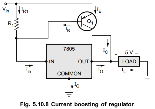
For
the low load currents (IL), the drop across R1 is
insufficient (less than 0.7 V) to conduct the transistor Q1. Hence
the entire load current is supplied by the regulator itself.
When
the load current IL increases, the drop across R1 also
increases, when it becomes greater than 0.7 V then the transistor Qi starts
conducting. For example if R1 is 7 Q then for load current above 100
mA, VR1 becomes 100 mA × 7 i.e. 0.7 V and Q1 starts
conducting. The excess current required by the regulator is supplied by Q1,
by amplifying IB as per the relation IC = β IB. Hence
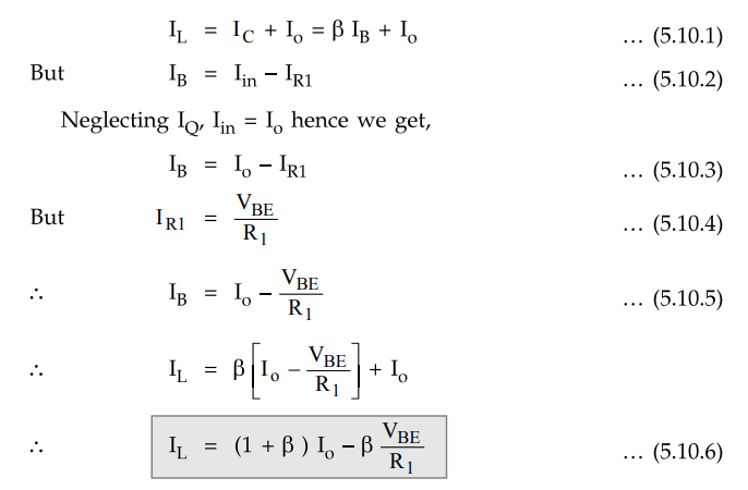
Thus
the current boosting is achieved which depends on the value of β and (Io)max of the
regulator.
Example
5.10. 2 For a 7805 IC voltage regulator, a current
boosting is provided with a transistor having VBE = 1 V and β = 15. Calculate maximum load current it can
deliver. Assume R1 as 7 Ω.
Solution
:
The (Io )max of 7805 regulator is 1 A.
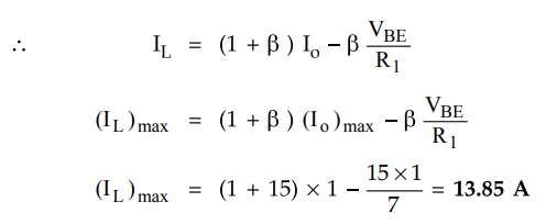
Thus
IC which can supply maximum of 1 A can supply maximum load of 13.85 A, with the
help of the current boosting arrangement.
Example
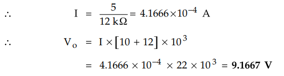
5.10. 3 The simplified block diagram of an 1C
voltage regulator is shown in Fig. 5.10.9. Calculate its output voltage Vo.
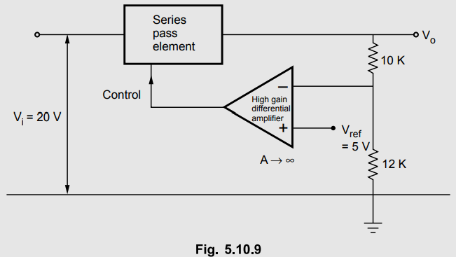
Solution
:
As the gain of differential amplifier A → ∞,
the virtual ground is applicable to it.
Hence
VB = Vref.
VB
=5V
This
is shown in the Fig. 5.10.9 (a).
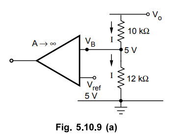
The
current I remains same through both the resistors as no current flows into the
op-amp.
Example
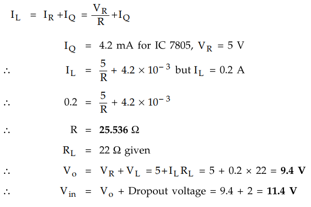
5.10.4 Using 7805 design a current source to deliver a
0.2 A current to a 22 Ohm 10 W load.
Solution
:
The current source using 7805 is shown in the Fig. 5.10.10.
The
current through RL is given by,
Review Questions
1. Explain the block
diagram of basic three terminal IC regulator.
2. Draw and explain
the typical connection of IC 7805.
3. How to achieve
adjustable regulator using 78XX series ?
4. How can the current
drive capability be increased while using three terminal voltage regulators ?
5. Draw the circuit
diagram and explain the operation of any one negative voltage regulator.
Dec.-07, Marks 8
6. What do you mean by
fixed voltage regulators ? List its applications.
Linear Integrated Circuits: Unit V: Application ICs : Tag: : Features, Functional Block Diagram, Performance parameters, Applications, Solved Example Problems - Three Terminal Fixed Voltage Regulators
Related Topics
Related Subjects

Linear Integrated Circuits
EE3402 Lic Operational Amplifiers 4th Semester EEE Dept | 2021 Regulation | 4th Semester EEE Dept 2021 Regulation