Linear Integrated Circuits: Unit IV: Special ICs
Timer IC 555
Operating working principle, Block Diagram, Pin Diagram, Functions of Pins, Symbol, Functional diagram, Waveform, Circuit Diagram, Solved Example Problems
The timer IC 555 is most versatile linear integrated device introduced by Signetics corporation in early 1970. It is basically a monolithic timer circuit which can be used in many applications such as monostable and astable multivibrators, linear ramp generator, missing pulse detector, pulse width modulator etc.
Timer IC 555
The
timer IC 555 is most versatile linear integrated device introduced by Signetics
corporation in early 1970. It is basically a monolithic timer circuit which can
be used in many applications such as monostable and astable multivibrators,
linear ramp generator, missing pulse detector, pulse width modulator etc.
The
IC 555 timer combines the following elements :
1)
A relaxation oscillator 2) R-S flip-flop
3)
Two comparators 4) Discharge
transistor
R-S
Flip-Flop
The Fig. 4.1.1 shows the part of the basic R-S flip-flop circuit. It uses a pair of cross-coupled transistors. Each collector drives the base of opposite transistor through a resistance RB. In such a circuit, one transistor operates in saturation while the other in cut-off region. Thus if the transistor Q2 is in saturation then its collector voltage is zero. This voltage is the base drive of transistor Q1. So there is no base drive for Q1 and it goes into cut-off. Thus its collector voltage is approximately +VCC. This drives the base of Q2 which ensures that the Q2 operates in saturation region.

Now
if transistor Q2 goes into cut-off, its collector voltage approaches
to +VCC which drives the transistor Q1 into saturation.
This makes collector voltage of Q1 almost zero which keeps the transistor Q2
in cut-off. So all the time, circuit ensures that one transistor operates in
saturation and other in cut-off.
The
two outputs Q and ![]() are taken from two collectors. Depending upon the
transistor operation, the output value gets decided.
are taken from two collectors. Depending upon the
transistor operation, the output value gets decided.
Now
this basic circuit along with some additional components gives us a popular R-S
flip-flop circuit. It has two inputs set (S) and reset (R). With the help of
these inputs, the output Q can be made high or low. Depending on Q,
complementary will be the value of output ![]() i.e. low or high.
i.e. low or high.
The
Fig. 4.1.2 shows the symbol of R-S flip-flop circuit. When input set (S) is
high, the output Q is high and ![]() is low. The high reset (R) input resets
the output Q to low. The output Q remains in its state of high or low unless
and until it is triggered externally into the opposite state.
is low. The high reset (R) input resets
the output Q to low. The output Q remains in its state of high or low unless
and until it is triggered externally into the opposite state.

The
Table 4.1.1 shows the state of output Q related to inputs S and R.

S
= Set, R = Reset, NC = No Change, * = Race
To
understand the operation of IC 555 timer, let us study the basic timing concept
using R-S flip-flop.
Basic
Timing Circuit
The
Fig. 4.1.3 shows the basic timing circuit, which uses R-S flip-flop along with
some other elements.

To
understand the operation, consider that the output Q is high. This drives the
base of Q1 and as it is high it drives Q1 into
saturation. It makes the capacitor voltage zero and as other end of capacitor
is grounded, the capacitor is shorted. In this condition it cannot be charged.
The
circuit uses a comparator. The noninverting input of comparator is called
threshold voltage. While its inverting input is called control voltage. The R1
and R2 forms a potential
divider which maintains control voltage constant at +10 V. As Q is high and
transistor Q1 is in saturation, the threshold voltage is zero.
As
R1 - 5 kΩ and R2 = 10 kΩ
Control
voltage = R2 / R1 + R2 × VCC = 10 /
5 + 10 × 15 = 10 V constant
Now
if high voltage is applied to the reset (R) input of flip-flop then it resets
R-S flip-flop and output Q goes low. This drives the transistor Q1
in cut-off. Now the capacitor is free to charge and starts charging through
resistance R. The threshold voltage thus starts increasing. When it becomes
just greater than +10 V which is the control voltage, the comparator output
goes high. This high signal is driving the set (S) input of R-S flip-flop. This
changes the state of output Q back to high. This drives transistor Q1
into saturation which quickly discharges the capacitor C.
The
Fig. 4.1.4 shows the waveforms of threshold voltage and output voltage Vout
The charging of capacitor is exponential hence the threshold voltage is also
exponential in nature. When Q goes low, the ![]() becomes high and positive
going pulse appears at Vout. Similarly when capacitor voltages increases more
than the control voltage, Q becomes high and
becomes high and positive
going pulse appears at Vout. Similarly when capacitor voltages increases more
than the control voltage, Q becomes high and ![]() becomes low. This
brings Vout to zero instantly. Thus a rectangular output gets produced.
becomes low. This
brings Vout to zero instantly. Thus a rectangular output gets produced.
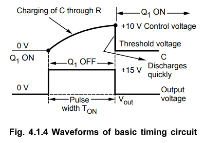
It
can be observed that output remains high for the time which is required by the
capacitor to charge upto control voltage, through R. Thus by varying R or C,
the output pulse width can be varied. This is the working principle of timer IC
555.
1. Block Diagram of IC 555
The
Fig. 4.1.5 (a) and (b) show the pin diagram and the block diagram of the IC NE
555 timer. This is 8 pin IC timer.

a.
Functions of Pins
The
pin numbers of IC 555 and their functions are discussed below :
Pin
1 : Ground
All
the voltages are measured with respect to this terminal.
Pin
2 : Trigger
The
IC 555 uses two comparators. The voltage divider consists of three equal
resistances. Due to voltage divider, the voltage of noninverting terminal of
comparator 2 is fixed at VCC/3. The inverting input of comparator 2
which is compared with VCC/3, is nothing but trigger input brought
out as pin number 2. When the trigger input is slightly less than VCC/3
the comparator 2 output goes high. This output is given to reset input of R-S
flip-flop. So high output of comparator 2 resets the flip-flop.
Pin
3 :
Output The complementary signal output (Q) of the flip-flop goes to pin
3 which is the output. The load can be connected in two ways. One between pin 3
and ground while other between pin 3 and pin 8.
Pin
4 : Reset This is an interrupt to the timing device. When pin
4 is grounded, it stops the working of device and makes it off. Thus, pin 4
provides on/off feature to the IC 555. This reset input overrides all other
functions within the timer when it is momentarily grounded.
Pin
5 : Control Voltage Input In most of the applications,
external control voltage input is not used. This pin is nothing but the
inverting input terminal of comparator 1. The voltage divider holds the voltage
of this input at 2/3 VCC. This is reference level for comparator 1
with which threshold is compared. If reference level required is other than 2/3
VCC for comparator 1 then
external input is to be given to pin 5.
If
external input applied to pin 5 is alternating then the reference level for
comparator 1 keeps on changing above and below 2/3 VCC. Due to this,
the variable pulse width output is possible. This is called pulse width
modulation, which is possible due to pin 5.
When
such control voltage is not required, a capacitor of 0.01 µF is connected
between pin 5 and ground. This capacitor bypasses noise or ripple content from
the supply.
Pin
6 : Threshold This is the noninverting input terminal
of comparator 1. The external voltage is applied to this pin 6. When this
voltage is more than 2/3 VCC, the comparator 1 output goes high.
This is given to the set input of R-S flip-flop. Thus high output of comparator
1 sets the flip-flop. This makes Q of flip-flop high and ![]() low. Thus
the output of IC 555 at pin 3 goes low.
low. Thus
the output of IC 555 at pin 3 goes low.
Remember
that output at pin 3 is ![]() which is complementary output of
flip-flop. In short,
which is complementary output of
flip-flop. In short,
For
threshold > 2/3 VCC, flip-flop → set, Q → high, output at pin 3 →
low
For
trigger < 1/3 VCC, flip-flop → reset, Q → low, output at pin 3 →
high
Pin
7 : Discharge This pin is connected to the collector
of the discharge transistor Qd. When the output is high then Q is low and
transistor Qd is off. It acts as an open circuit to the external
capacitor C to be connected across it, so capacitor C can charge as described
earlier. When output is low, Q is high which drives the base of Qd
high, driving transistor Qd in saturation. It acts as short circuit,
shorting the external capacitor C to be connected across it.
Pin
8 : Supply +VCC
The
IC 555 timer can work with any supply voltage between 4.5 V and 16 V.
2. Monostable Multivibrator using IC 555
The
IC 555 timer can be operated as a monostable multivibrator by connecting an
external resistor and a capacitor as shown in the Fig. 4.1.6.

The
circuit has only one stable state. When trigger is applied, it produces a pulse
at the output and returns back to its stable state. The duration of the pulse
depends on the values of R and C. As it has only one stable state, it is called
one shot multivibrator.
a.
Operation
The
flip-flop is initially set i.e. Q is high. This drives the transistor Qd
in saturation. The capacitor discharges completely and voltage across it is
nearly zero. The output at pin 3 is low.
When
a trigger input, a low going pulse is applied, then circuit state remains
unchanged till trigger voltage is greater than 1/3 VCC. When it
becomes less than 1/3 Vcc, then comparator 2 output goes high. This resets the
flip-flop so Q goes low and ![]() goes high. Low Q makes the transistor Qd
off. Hence capacitor starts charging through resistance R, as shown by dark
arrows in the Fig. 4.1.6.
goes high. Low Q makes the transistor Qd
off. Hence capacitor starts charging through resistance R, as shown by dark
arrows in the Fig. 4.1.6.
The voltage across capacitor increases exponentially. This voltage is nothing but the threshold voltage at pin 6. When this voltage becomes more than 2/3 Vcc, then comparator 1 output goes high. This sets the flip-flop i.e. Q becomes high and Q low. This high Q drives the transistor Qd in saturation. Thus capacitor C quickly discharges through Qd as shown by dotted arrows in the Fig. 4.1.7.
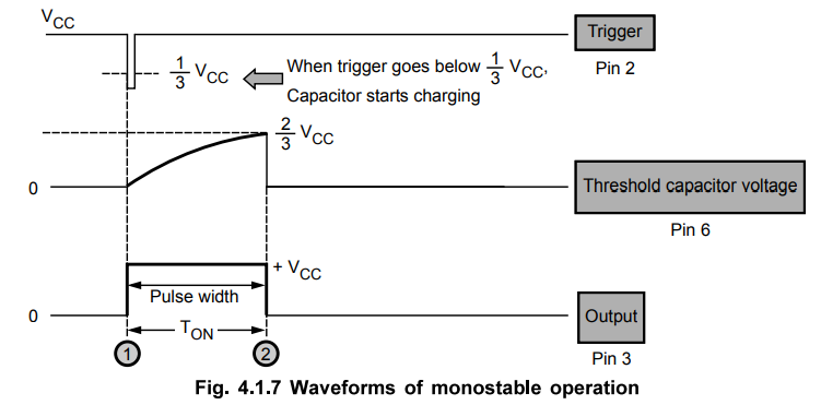
So
it can be noted that Vout at pin 3 is low at start, when trigger is less than
1/3 Vcc it becomes high and when threshold is greater than 2/3 VCc again
becomes low, till next trigger pulse occurs. So a rectangular wave is produced
at the output. The pulse width of this rectangular pulse is controlled by the
charging time of capacitor. This depends on the time constant RC. Thus RC controls
the pulse width. The waveforms are shown in the Fig. 4.1.7.
b.
Derivation of Pulse Width
The
voltage across capacitor increases exponentially and is given by,
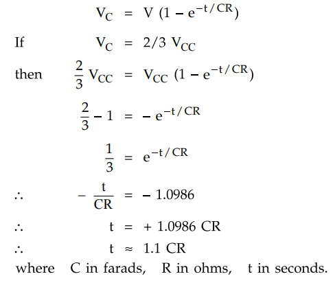
Thus,
we can say that voltage across capacitor will reach 2/3 VCC in approximately
1.1 times, time constant i.e. 1.1 RC.
Thus
the pulse width denoted as W is given by,
W
= 1.1 RC

c.
Schematic Diagram
Generally
a schematic diagram of the IC 555 circuits is shown which does not include
comparators, flip-flop etc. It only shows the external components to be connected
to the 8 pins of IC 555. Thus, the schematic diagram of IC 555 as a monostable
multivibrator is shown in the Fig. 4.1.9.
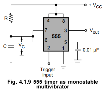
The
external components R and C are shown. To avoid accidental reset, pin 4 is
connected to pin 8 which is supply +Vcc. To have the noise filtering of control
voltage, the pin 5 is grounded through a small capacitor of 0.01 μF.
d. Applications of Monostable Multivibrator
1.
Frequency Divider
We
know that, in monostable multivibrator, application of trigger pulse gives a
positive going pulse on the output. The same monostable circuit can be used as
a frequency divider if the timing interval is adjusted to be longer than the
period of the input signal, as shown in the Fig. 4.1.10.

Key
Point Here, timing interval ‘t’ is kept slightly
larger than the time period T of the trigger input signal.
The
monostable multivibrator will be triggered by the first negative going edge of
the trigger input, which will make output to go in its high state. The output
will remain high for the period equal to 'timing interval'. As timing interval
is greater than time period of the trigger input, output will still be high
when the second negative going pulse occurs. The monostable will, however, be
re-triggered on the third negative-going pulse. Therefore, monostable triggers
on every other pulse of the trigger input, so there is only one output for
every two input pulses, thus trigger signal is, divided by 2.
Key
Point In this way, by adjusting the timing interval,
the monostable circuit can be made integral fractions of the frequency of the
input trigger signal.
2.
Pulse Width Modulation
The Fig. 4.1.11 shows pulse width modulator.

It is basically a monostable
multivibrator with a modulating input signal applied at the control voltage
input (pin 5). Internally, the control voltage is adjusted to the 2/3 VCC.
Externally applied modulating signal changes the control voltage and hence the
threshold voltage level of the upper comparator (comparator 1). As a result,
time period required to charge the capacitor upto threshold voltage level
changes, giving pulse width modulated signal at the output as shown in the Fig.
4.1.12.

Key
Point It may be noted from the output waveform that
the pulse duration varies according to the modulating signal level, but the
frequency of the output pulses is same as that of the trigger input signal.
3.
Linear Ramp Generator
When
a capacitor is charged with a constant current source then linear ramp is
obtained. This concept is used in linear ramp generator. The circuit is shown
in the Fig. 4.1.13.
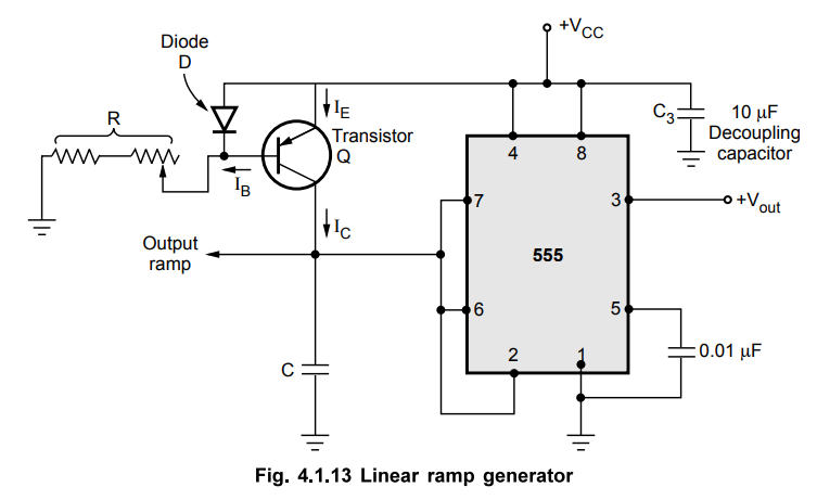
The
circuit is used to obtain constant current Ic is a current mirror circuit,
using transistor Q and diode D. The current IC, charges capacitor C
at a constant rate towards + VCC. But when voltage at pin 6 i.e.
capacitor voltage VC becomes (2/3 Vcc), the comparator makes
internal transistor Q1 ON within no time. But while discharging when
VC becomes (1/3 VCC), the second comparator makes Q1
OFF and C starts its charging again.
As discharging time of capacitor C is very small, the time period of ramp is
assumed practically same as that of charging time of capacitor.
The
waveforms are shown in the Fig. 4.1.14.
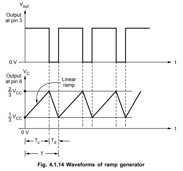
The
time period of the ramp is approximately given by,

4.
Missing Pulse Detector
The
Fig. 4.1.15 (a) shows the circuit diagram for missing pulse detector. When
signal input is at ground level (0 V), the emitter diode of transistor T
forward biases and clamps capacitor voltage VC to 0.7 V. This forces
output voltage to stay in its high state. When signal input goes high, the
transistor cuts off and capacitor C begins to charge. If input signal again
goes low before the 555 completes its timing cycle, the voltage across C is
reset to 0.7 V. If, however, input signal does not go low before the 555
completes its timing cycle, the 555 enters its normal state and output voltage
goes low. This is illustrated in Fig. 4.1.15 (b).
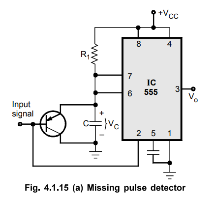
For
this circuit timing interval is adjusted such that it is slightly longer than
the period of input signal. The continuous low going pulses of the period less
than the timing interval do not allow capacitor to charge upto 2/3 VCC.
AS a result, output voltage remains high. In case of missing pulse (pulse 4),
capacitor charges upto 2/3 VCC and forces output voltage in to its low state,
as shown in the Fig. 4.1.15 (b). This type of circuit can be used to detect a
missing heart beat.

5.
Pulse Position Modulation (PPM)
In
pulse position modulation, the amplitude and width of the pulses are kept
constant, while the position of each pulse with reference to the position of a
reference pulse, is changed according to the instantaneous sampled value of the
modulating signal.
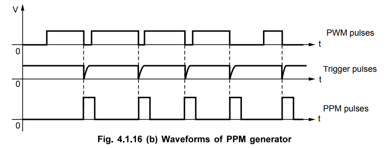
The Fig. 4.1.16 (a) shows the PPM generator.

It consists of differentiator and a monostable multivibrator. The input to the differentiator is a PWM waveform. The differentiator generates positive and negative spikes corresponding to leading and trailing edges of the PWM waveform. Diode Dx is used to bypass the positive spikes. The negative spikes are used to the trigger monostable multivibrator. The monostable multivibrator then generates the pulses of same width and amplitude with reference to trigger to give pulse position modulated waveform, as shown in the Fig. 4.1.16 (b).
Example
4.1.1 Draw the circuit diagram of timer using IC 555.
Calculate the component values if the controlled door should remain open for 15
secs after a trigger signal is received. The d.c. voltage available is either
10 or 15 volts.Example 4.1.1
Solution : The requirement is that the door must be open for 15 sec after receiving a trigger signal and then gets shut down automatically. This requires IC 555 in a monostable mode with a pulse width of 15 sec
W
= 15 sec
Now W = 1.1 RC
15
= 1.1 RC
Choose
C = 100 µF
R
= 136.363 kΩ
The
designed circuit is shown in the Fig. 4.1.17.

The
supply voltage 10 or 15 V has no effect on the operation of the circuit or the
values of R and C selected.
Example
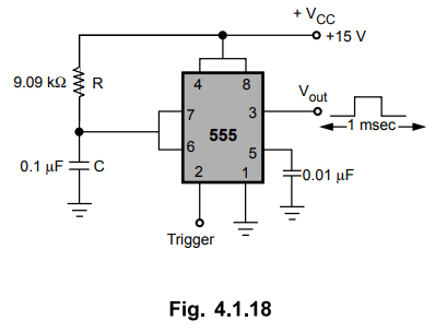
4.1.2 Design a monostable multivibrator for a time delay
of 1 msec using the IC 555.
Solution
:

The
designed circuit is shown in the Fig. 4.1.18.
Example
4.1.3 Design a monostable multivibrator using IC 555 timer
to produce a quasistable state duration of 200 ms. Select suitable trigger
signal. Draw the input and output waveforms and mark the necessary timings.
Solution
:
W = 200 ms
For
monostable operation,

The Circuit is shown in the Fig. 4.1.19.

The
waveforms of trigger signal, output and threshold capacitor voltage is shown in
the Fig. 4.1.20.

Thus
if VCC = + 15 V then the
trigger input is 1/3 VCC i.e. 5 V.
3. Astable Multivibrator using IC 555
The
Fig. 4.1.21 shows the IC 555 connected as an astable multivibrator. The
threshold input is connected to the trigger input. Two external resistances RA,
RB and a capacitor C is used in the circuit.
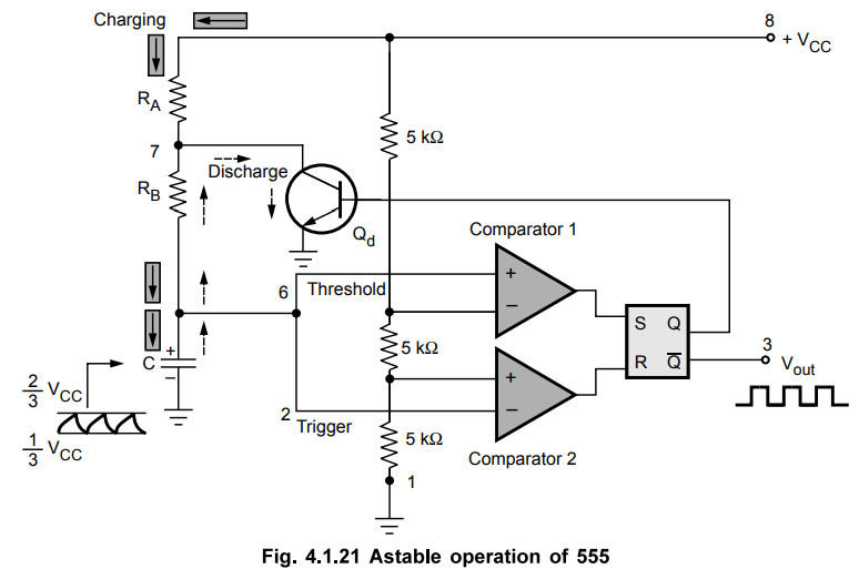
This
circuit has no stable state. The circuits changes its state alternately. Hence
the operation is also called free running nonsinusoidal oscillator.
1.
Operation
When
the flip-flop is set, Q is high which drives the transistor Qd in
saturation and the capacitor gets discharged. Now the capacitor voltage is
nothing but the trigger voltage. So while discharging, when it becomes less
than 1/3 VCC, comparator 2 output goes high. This resets the
flip-flop hence Q goes low and ![]() goes high.
goes high.
The
low Q makes the transistor off. Thus capacitor starts charging through the
resistances RA, RB and VCC. The charging path
is shown by thick arrows in the Fig. 4.1.22. As total resistance in the
charging path is (RA + RB), the charging time constant is
(RA + RB) C.
Now
the capacitor voltage is also a threshold voltage. While charging, capacitor
voltage increases i.e. the threshold voltage increases. When it exceeds 2/3 VCC,
then the comparator 1 output goes high which sets the flip-flop. The flip-flop
output Q becomes high and output at pin 3 i.e. ![]() becomes low. High Q
drives transistor Qd in saturation and capacitor starts discharging
through resistance RB and transistor Qd. This path is
shown by dotted arrows in the Fig. 4.1.22. Thus the discharging time constant
is RBC. When capacitor voltage becomes less than 1/3 VCC,
comparator 2 output goes high, resetting the flip-flop. This cycle repeats.
becomes low. High Q
drives transistor Qd in saturation and capacitor starts discharging
through resistance RB and transistor Qd. This path is
shown by dotted arrows in the Fig. 4.1.22. Thus the discharging time constant
is RBC. When capacitor voltage becomes less than 1/3 VCC,
comparator 2 output goes high, resetting the flip-flop. This cycle repeats.
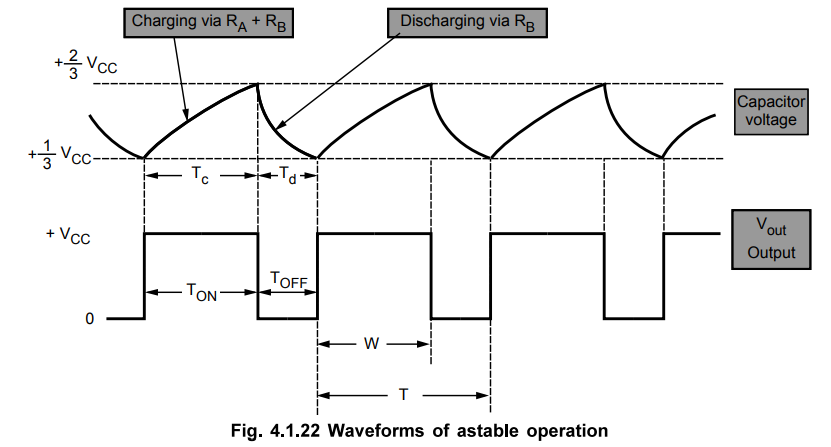
Thus
when capacitor is charging, output is high while when it is discharging the
output is low. The output is a rectangular wave. The capacitor voltage is exponentially
rising and falling. The waveforms are shown in the Fig. 4.1.22.
b.
Duty Cycle
Generally
the charging time constant is greater than the discharging time constant. Hence
at the output, the waveform is not symmetric. The high output remains for longer
period than low output. The ratio of high output period and low output period
is given by a mathematical parameter called duty cycle. It is defined as the
ratio of ON time i.e. high output to the total time of one cycle. As shown in
the Fig. 4.1.22.
W
= Time for output is high = TON
T
= Time of one cycle
D
= Duty cycle = W / T
%D = W / T × 100 %
The
charging time for the capacitor is given by,
Tc
= Charging time - 0.693 (RA + RB) C
While
the discharge time is given by,
Td
= Discharging time - 0.693 RB C
Hence
the time for one cycle is,

If RA is much smaller than RB, duty cycle approaches to 50% and output waveform approaches to square wave.
c.
Schematic Diagram
The
Fig. 4.1.23 shows the schematic diagram of astable timer circuit. It shows only
the external components RA, RB and C. The pin 4 is tied
to pin 8 and pin 5 is grounded through a small capacitor.
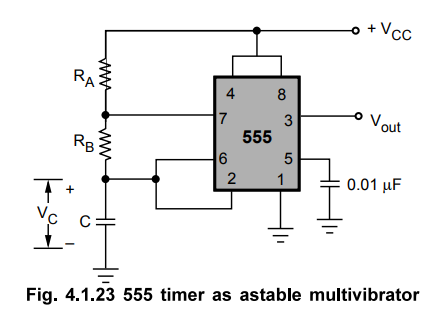
The
important application of astable multivibrator is voltage controlled oscillator
(VCO).
Example
4.1.4 In the astable multivibrator using 555 timer, RA
= 2.2 kΩ, RB = 6.8 kΩ, and C - 0.01 µF. Calculate tHIGH,
tLOW, free running frequency and duty cycle.
May-15,
Marks 8
Solution
:
RA = 2.2 kΩ, RB = 2.2 kΩ, C = 0.01 µF

d.
Applications of Astable Multivibrator
1.
Square Wave Generator
It
can be observed from the expression of duty cycle that in astable operation
exact 50 % duty cycle is not possible to achieve. To get exactly 50 % duty
cycle i.e. square wave output it is necessary to modify the astable timer
circuit.
The
modified astable circuit used to obtain the square wave output is shown in the
Fig. 4.1.24.
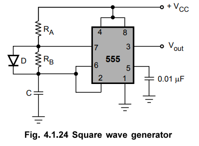
In
the modified circuit, the capacitor C charges through RA and diode D and
discharges through RB. To obtain square wave (50 % duty cycle)
resistance RB is adjusted such that it is equal to the summation
of resistance RAand the forward
resistance of diode D. Usually, potentiometer is used for exact adjustments of
resistors.
The
waveforms of square wave generator are shown in the Fig. 4.1.25.

The
other applications are,
1. Voltage controlled oscillator, 2. FSK generator, 3. Flasher circuit.
2.
Voltage Controlled Oscillator (VCO)
The
Fig. 4.1.26 shows the circuit diagram for voltage controlled oscillator. It is
basically an astable multivibrator circuit with variable control voltage.

We
know that internally set voltage at the control voltage terminal is 2/3 VCC
. In this circuit, the control voltage
is externally set by the potentiometer. With change in the control voltage, the
upper threshold voltage changes and thus the time required C to charge
capacitor upto upper threshold voltage changes. Similarly, discharge time .
also changes. As a result, the frequency of the output voltage changes.
If
control voltage is increased, the capacitor will take more time to charge and
discharge and therefore frequency will decrease. On the otherhand, if control
voltage is decreased, the capacitor will take less time to charge and
discharge, increasing the frequency of the output signal. Thus by varying
control voltage we can change the frequency
3.
FSK Generator
Binary
code consists of l's and 0's. It can be Digital transmitted by shifting a input
carrier frequency. One fix frequency represents one and other represents zero. This
type of transmission if called Frequency Shift Keying (FSK) technique. Astable
multivibrator using 555 can be used to generate FSK signal.
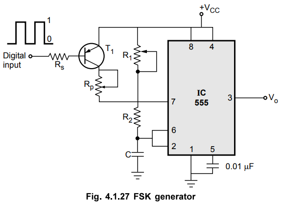
The
circuit for FSK generation is as shown in the Fig. 4.1.27.
When
digital input is HIGH (logic 1), transistor T1 is OFF and 555 timer
works in a normal astable mode. The frequency of the output waveform can be
given as

When
input is LOW (logic 0), transistor T1 is ON and connects the resistance Rp in
parallel with R1. With this connecting effective Rleft
becomes R1 || Rp, and output frequency is now given by
with
this connection effective resistance Reff becomes R1 || Rp,
Example
4.1.5 Design an astable multivibrator which will flash
the electric bulb such that its ON time will be 3 seconds and off time will be
1 seconds.
Solution
:
Fig. 4.1.28 shows astable circuit used to drive relay

This relay should be energized for 3 seconds and
then de-energize by 1 seconds. Hence charging time of capacitor is 3 seconds
which is a pulse width W.
W
= 3 seconds
While
total time of one cycle is,
T
= 3 + 1 = 4 seconds

The
values are not standard but can be adjusted using the potentiometers.
d.
Astable Multivibrator with a Variable Duty Cycle
Generally
astable mode of IC 555 is used to obtain the duty cycle between 50 % to 100 %.
But if duty cycle less than 50 % is required, the circuit can be modified as
shown in the Fig. 4.1.29.
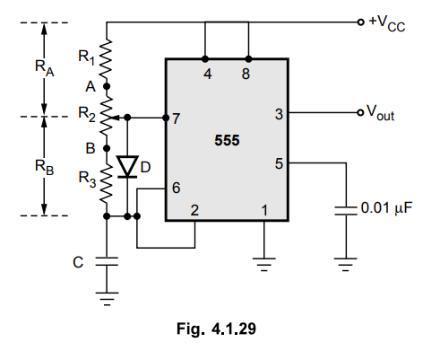
The
circuit is similar to square wave generator, but instead of connecting diode
across fixed RB it is connected across a combination of variable R2
and R3. The resistance R2 is variable and it can be added to R1
or R3 to change the charging and discharging resistance. Thus a
variable duty cycle can be achieved.
The
charging time for the capacitor is,
Tc
= (R1 + Part of R2) 0.693 C
The
discharging time for the capacitor is,
Td
= (R3 + Remaining part of R2) 0.693 C
T
= Tc + Td = 0.693 C [R1 + R2 + R3]
f
= 1 / T = 1.44 / (R1 + R2 + R3) C
Range
of duty cycle possible :
Let
position of R2 potentiometer is A i.e. part of R2 in
series with R1 is zero and entirely R2 gets added to R3
Thus
minimum duty cycle, less than 50 % is possible.
For
R2 potentiometer position at B, maximum duty cycle is possible.
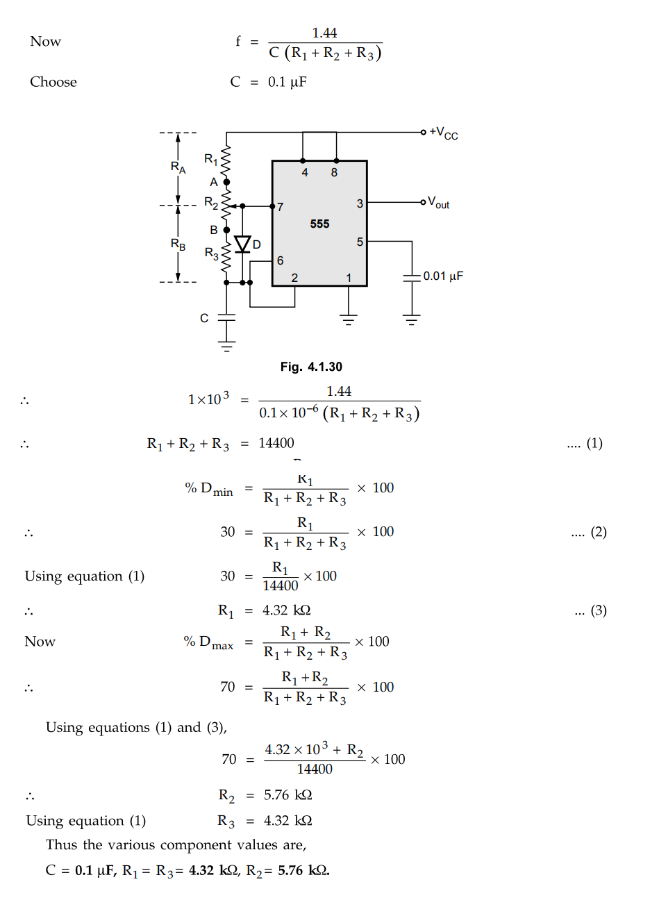
Example
4.1.6 Design an astable multivibrator for an output
frequency of 1 kHz but a variable duty cycle of 30 % to 70 %. Assume VCC
= 12 V.
Solution:
For variable duty cycle, use the modified circuit as shown in the Fig. 4.1.30.
Example
4.1.7 Draw the circuit diagram of an astable
multivibrator to generate the output signal with frequency of 1 kHz and the
duty cycle of 75 %.
Solution
:

Hence
the circuit diagram is as shown in the Fig. 4.1.31.

Example
4.1.8 A 555 timer configured in astable mode with RA
= 2 kohm, RB = 4 kohm and C = 0.1 µ.F. Determine the frequency of
the ouptut and duty cycle.
Solution
: This
is astable mode of operation.

Example
4.1.9 Design and draw the waveforms of 1 kHz square
waveform generator using 555 timer for duty cycle, i) D = 25 % ii) D =
50 %
Solution
:

As
D is less than 50 %, modified circuit is used.
The
circuit is shown in the Fig. 4.1.32.

Choose
C - 0.1 µF
The
charging of C takes place through RA and didoe D while the
discharging of C takes place through RB only.
Assuming
ideal diode,
TON
= 0.69 RAC and TOFF = 0.69 RBC
RA
= 3.62 kΩ and RB = 10-.869 kΩ
The
output waveform is shown in the Fig. 4.1.34 (a),
ii)
D = 50 %, f = 1 kHz
T
= 1 ms, For D = 50 %, Td = Tc = 0.5 ms
The
circuit is shown in the Fig. 4.1.33.
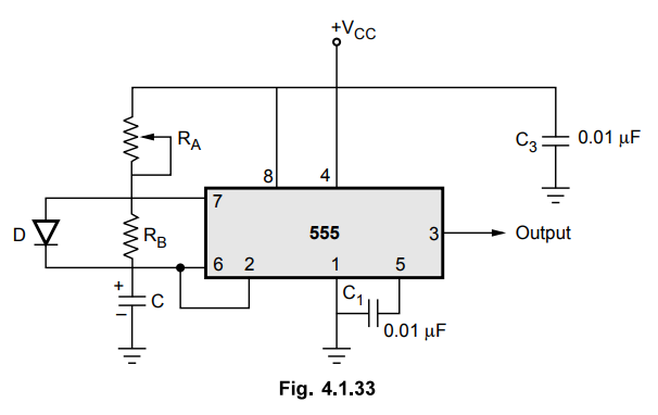
Choose
C = 0.1 µF
Td
= 0.69 RAC while Tc = 0.69 RBC
But
Td = Tc = 0.5 ms hence RA = RB =
7.246 kΩ with potentiometer, perfect square wave can be obtained. The output
waveform is shown in the Fig. 4.1.34 (b).

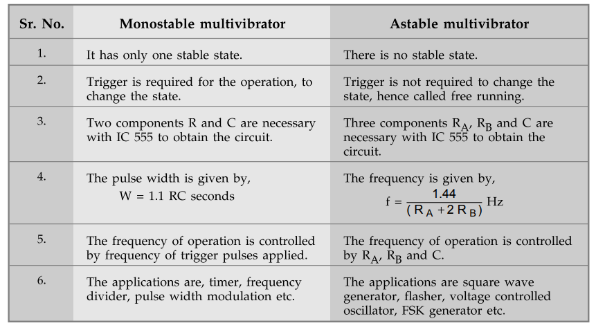
4. Comparison of Multivibrator Circuits
5. Bistable Multivibrator using IC 555
The
Fig. 4.1.35 shows IC 555 in a bistable mode.

The
bistable mode has two stable states, high and low.
As
shown in the circuit, pin 6 is not connected hence no voltage is present at pin
6. Thus threshold is never reached hence output remains high indefinitely when
SET switch is pressed. Operating SET switch, the output goes into high state
till RESET switch is operated.
Making
RESET switch closed, pin 4 gets connected to ground creating low pulse which
resets the IC 555 and output goes low. This remains low, till SET switch is
closed again.
When
SET is closed, pin 2 gets connected to ground. This causes the voltage to
bypass pin 2 which results into low pulse, triggering IC 555, making output
high. Thus SET is also called TRIGGER.
There
is no timing involved in this circuit hence no equations are needed to workout
the components.
The
waveforms are shown in the Fig. 4.1.36. The circuit is extensively used in
computers and other digital circuits.

6. Features of IC 555 Timer
The
various features of the IC 555 timer are :
1.
The 555 is a monolithic timer device which can be used to produce accurate and
highly stable time delays or oscillation. It can be used to produce time delays
ranging from few microseconds to several hours.
2.
It has two basic operating modes : Monostable and astable.
3.
It is available in three packages : 8-pin metalcan, 8-pin mini DIP or a 14-pin
DTP. A 14-pin package is IC 556 which consists of two 555 timers.
4.
The NE 555 (Signetics) can operate with a supply voltage in the range of 4.5 V
to 18 V and is capable of sourcing and sinking output currents of 200 mA. Its
CMOS version (TLC 555) can operate over a supply range of 2 V to 18 V and has
output current sinking and sourcing capabilities of 100 mA and 10 mA,
respectively.
5.
It has a very high temperature stability, as it is designed to operate in the
temperature range of -55 °C to 125 °C
6.
Its output is capatible with TTL, CMOS and Op-amp circuits.
7. 555 Timer as a Schmitt Trigger
The
Fig. 4.1.37 shows the use of 555 timer as a Schmitt trigger.

The
input is given to the pins 2 and 6 which are tied together. Pins 4 and 8 are
connected to supply voltage +VCC. The common point of two pins 2 and
6 is externally biased at VCC /2 through the resistance network R1
and R2. Generally R1 = R2 to get the biasing
of VCC/2. The upper comparator will trip at 2/3 VCC while
lower comparator at 1/3 VCC. The bias provided by R1 and R 2 is
centred within these two thresholds.
Thus
when sine wave of sufficient amplitude, greater than VCC/6 is applied to the
circuit as input, it causes the internal flip-flop to alternately set and
reset. Due to this, the circuit produces the square wave at the output, as shown
in the Fig. 4.1.38.

The
frequency of square wave remains same as that of input. The Schmitt trigger can
operate with the input frequencies upto 50 kHz.
Review Questions
1. Describe the
monostable operation of 555 timer.
2. Derive the
expression for the time delay of a monostable multivibrator using timer 555.
May-10, Marks 16
3. Draw the functional
diagram of astable multivibrator using IC 555 timer and explain its operation
and derive the expression for the frequency.
Dec.-03, 11, 12, 14,
Marks 16, May-08, 15, 16, Marks 8
4. Explain the
operation of square wave generator using IC 555 by drawing capacitor and output
voltage waveforms.
5. List the important
features of 555 timer.
6. Discuss two basic
modes in which IC 555 timer operates.
7. Draw the circuit of
a Schmitt trigger using 555 timer and explain its operation.
8. Briefly explain the
differences between the two operating modes of 555 timer.
Dec.-07, 17, Marks 10
9. Draw and explain
the functional diagram cf IC 555 timer.
10. Explain the
bistable operation of IC 555 with necessary waveforms.
11. Determine the
output pulse width cf the monostable multivibrator using IC 555, if
R = 12 kΩ. and C = 0.1
µF.
[Ans.: 1.32 ms]
12. A IC 555 timer
used as a monostable has R = 20 kΩ. and C = 0.01 pF. What is the duration of
output pulse ?
[Ans.: 0.22 ms]
13. A 555 timer is
configured to run in astable mode with R2 = 20 kΩ and R2 = 8 kΩ and
C = 0.1 µF. Determine
the output frequency and duty cycle.
[Ans.: 400 Hz, 77.77
%]
14. Design an astable
multivibrator using 555 timer to produce a 1 kHz square waveform for duty cycle
D = 0.50.
15. State the
applications of astable multivibrator using IC 555.
16. Design a 555 based
square wave generator to produce a symmetrical square wave of 2 kHz. If VCC
= 12 volts, draw the voltage across timing capacitor and the output ?
17. Design an astable
multivibrator having a duty cycle of 40 % with a frequency of 1 kHz. Use 555
timer.
[Ans.: C = 0.01 µF, RA
= 57.72 kΩ, RB = 86.58 kΩ]
18. Discuss the operation of FSK generator using 555 timer.
Linear Integrated Circuits: Unit IV: Special ICs : Tag: : Operating working principle, Block Diagram, Pin Diagram, Functions of Pins, Symbol, Functional diagram, Waveform, Circuit Diagram, Solved Example Problems - Timer IC 555
Related Topics
Related Subjects

Linear Integrated Circuits
EE3402 Lic Operational Amplifiers 4th Semester EEE Dept | 2021 Regulation | 4th Semester EEE Dept 2021 Regulation