Microprocessors and Microcontrollers: Unit V: (b) Introduction to RISC Based Architecture
Timers
Introduction to RISC Based Architecture
1. Registers used for Timer/Counter Operation 2. Prescaling of PIC18 Timers 3. Timer 0 4. Timer 1 5. Timer 2 6. Timer 3 7. Delay Calculations
Timers
1. Registers used for Timer/Counter Operation
•
PIC18 has two to five timers depending on the PIC family it belongs to. They
are Timer 0, 1, 3, 4 and 5. PIC18F458 has four timers: Timer 0, Timer 1, Timer
2, and Timer 3.
•
They can be used either as timers to generate time delays or as counters to
count events.
•
In PIC18F458, timers 0, 1 and 3 are 16-bit timers while timer 2 is 8-bit timer.
These timers can be used as timer, counters or for PWM generation.

•
Selecting clock source clock source can be internal or external and is
controlled by bit TxCS:
■
D TxCS = 0: Clock source is internal and is taken from Fosc/4.
■
TxCS
= 1: Clock source is external and is taken from TxCKI pin; in this case TXSE
controls the edge of the signal which triggers increment.
■
Note:
x can be 0, 1, 2 or 4.
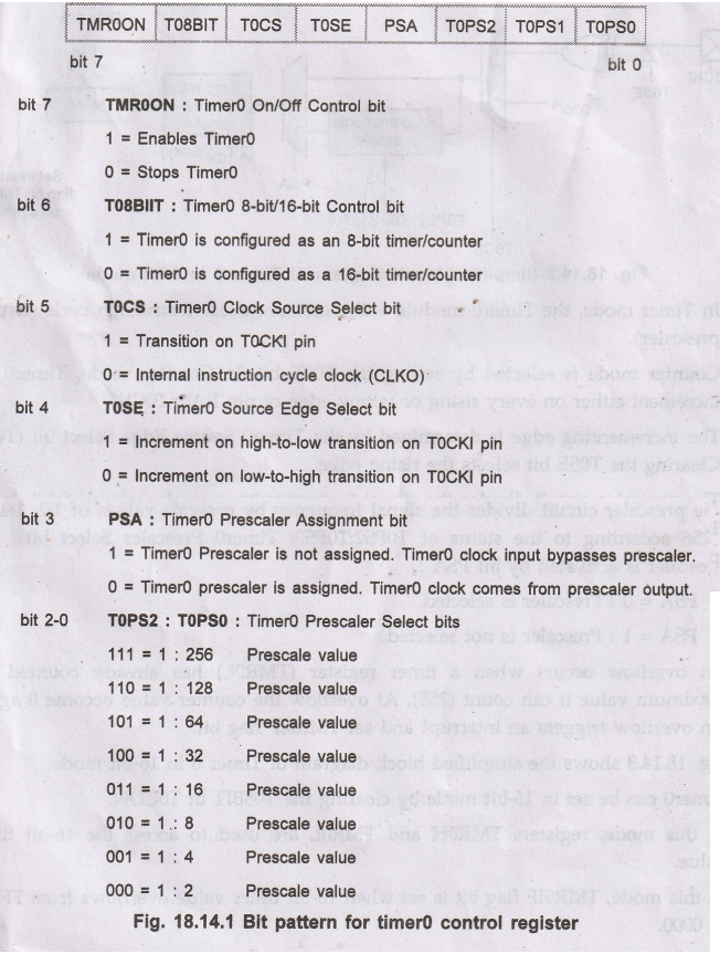
2. Prescaling of PIC18 Timers
•
In some cases, the clock coming from the oscillator could be too fast for an
application. We can lower it by using the frequency prescaler.
•
Timer 0 : The prescaler circuit divides the signal frequency by prescale
values of 1:2, 1: 4, ..., 1: 256 according to the status of TOPS2: TOPSO:
Timero Prescaler Select bits. The prescaler is activated by bit PSA:
■
PSA
= 0 Prescaler is selected.
■
PSA
1 = Prescaler is not selected.
•
Timer 1: The prescaler circuit divides the signal frequency
by prescale values of 1:1, 1:2, 1: 4, 1:8 according to the status of T1CKPS1:T1CKPS0:
Timer1 Input Clock Prescale Select bits.
•
Timer 2: The prescaler circuit divides the signal frequency
by prescale values of 11, 14, 1: 16 according to the status of T2CKPS1:T2CKPS0:
Timer2 Clock Prescale Select bits.
•
Timer 3: The prescaler circuit divides the signal frequency
by prescale values of 1:1, 1:2, 1:4, 1: 8 according to the status of T3CKPS1:T3CKPS0:
Timer3 Input. Clock Prescale Select bits.
3. Timer 0
a.
Features
•
The
features of Timer 0 are:
1.
Software selectable as an 8-bit or 16-bit timer/counter.
2.
Readable and writable
3.
Dedicated 8-bit software programmable prescaler
4.
Clock source selectable to be external or internal
5.
Interrupt-on-overflow from FFh to 00h in 8-bit mode and FFFFh to 0000h in
16-bit mode MCALAT
6.
Edge select for external clock
b.
T0CON: Timer0 Control Register
•
Fig. 18.14.1 shows the Timer0 Control register (T0CON). It is an 8-bit,
read/write register used to that controls all the aspects of Timer0 including:
enable/disable timer0, select the operating mode, select the clock source and
its transition (HIGH to LOW or LOW to HIGH), enable/disable prescaler and to
select the prescaler value if enabled.
c.
Block Diagram
•
Fig. 18.14.2 shows the simplified block diagram of Timer 0 in 8-bit mode.
•
Upon Reset, Timer0 is enabled in 8-bit mode with clock input from TOCKI maximum
prescale.
•
Timer0 can operate as a timer or as a counter. Timer mode is selected by
clearing the T0CS bit.
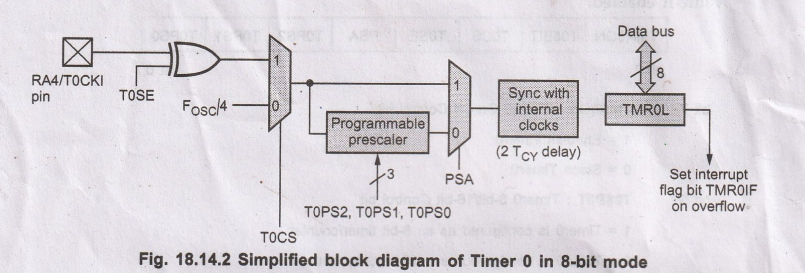
•
In Timer mode, the Timer0 module will increment every instruction cycle
(without prescaler).
•
Counter mode is selected by setting the T0CS bit. In Counter mode, Timer0 will
increment either on every rising or falling edge of pin RA4/T0CKI.
•
The incrementing edge is determined by the Timer0 Source Edge Select bit (T0SE).
Clearing the TOSE bit selects the rising edge.
•
The prescaler circuit divides the signal frequency by prescale values of 1:2,
1:4, ..., 1:256 according to the status of TOPS2:TOPSO: Timer0 Prescaler Select
bits. The prescaler is activated by bit PSA :
•
PSA = 0: Prescaler is selected.
•
PSA 1 Prescaler is not selected.
•
An overflow occurs when a timer register (TMROL) has already counted the
maximum value it can count (255). At overflow the counter value become 0 again.
An overflow triggers an interrupt and set TMR0IF flag bit.
•
Fig. 18.14.3 shows the simplified block diagram of Timer 0 in 16-bit mode.
•
Timer0 can be set in 16-bit mode by clearing the T08BIT in T0CON.
•
In this mode, registers TMR0H and TMR0L are used to access the 16-bit timer
value.
•
In this mode, TMR0IF flag bit is set when 16-bit timer value overflows from
FFFFh to 0000.
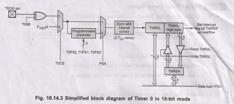
• Here, TMROH is not the high byte of the timer/counter in 16-bit mode, but is actually a buffered version of the high byte of Timer0. This is illustrated in Fig. 18.14.2.
d.
Applications
•
Applications of Timer0 are:
■
Generate wide range of accurate time delays by selecting the appropriate
prescaler options.
■
Measure
frequency of an unknown signal. det bra sal
4. Timer 1
a.
Features
•
The features of Timer 1 are :
1.
16-bit timer/counter
2.
Two 8-bit registers: TMR1H and TMR1
3.
Readable and writable (both registers)
4.
Internal or external clock select
5.
Interrupt-on-overflow from FFFFh to 0000h
6.
Reset from CCP module special event trigger
7.
Can not be disabled by SLEEP instruction
b.
T1CON: Timer1 Control Register
•
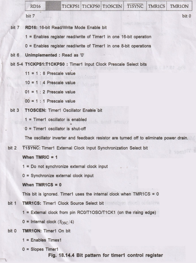
Fig. 18.14.4 shows the Timer1 Control register (T1CON). It is an 8-bit,
read/write register used to that controls all the aspects of Timer1.
c.
Block Diagram
Fig.
18.14.5 shows the simplified block diagram of Timer 1.

•
Timer1 can be enabled/disabled by setting/clearing control bit, TMR1ON (T1CON
register).
•
The operating mode for the Timer1 is determined by the clock select bit, TMRICS
(T1CON register). Timer1 can operate in one of these modes :
■
As a timer
■
As
a synchronous counter
■
As
an asynchronous counter
•
When TMR1CS=0: Timer1 increments every instruction cycle.
•
When TMR1CS = 1: Timer1 increments on every rising edge of the external clock
input or the Timer1 oscillator, if enabled.
•
When the Timer1 oscillator is enabled (T1OSCEN is set), the T1OSI and
T1OSO/T1CKI pins become inputs. This oscillator is a low power oscillator and
it is utilized in the sleep mode. In the sleep mode, the Timer1 is not disabled
and hence it can be used to implement the-chip real time clock (RTC).
•
Timer1 also has an internal "Reset input". This Reset can be
generated by the CCP module.
•
The prescaler circuit divides the signal frequency by prescale values of 1:1,
1:2, 1:4, 1:8 according to the status of T1CKPS1:T1CKPS0: Timer1 Input Clock
Prescale Select bits.
•
Here, TMR1IF flag bit is set when 16-bit timer value in TMR1 register pair
(TMR1H:TMR1L) increments from 0000h to FFFFh and rolls over to 0000h.
d.
Applications
•
Applications of Timer1 are :
■
Generate
accurate time delays by selecting the appropriate prescaler options.
■
Measure
frequency of an unknown signal.
■
Implement Real Time Clock (RTC)
■
Generate
special event trigger in compare mode of CCP module.
5. Timer 2
a.
Features
•
The features of Timer 2 are:
1.
8-bit timer (TMR2 register)
2.
8-bit period register (PR2)
3.
Readable and writable (both registers)
4.
Software programmable prescaler (1: 1, 1:4, 1:16)
5.
Software programmable postscaler (1 : 1 to 1 : 16)
6.
Interrupt on TMR2 match of PR2
7.
SSP module optional use of TMR2 output to generate clock shift
b.
T2CON: Timer2 Control Register
•
Fig. 18.14.6 shows the Timer1 Control register (T2CON). It is an 8-bit,
read/write register used to that controls all the aspects of Timer2.
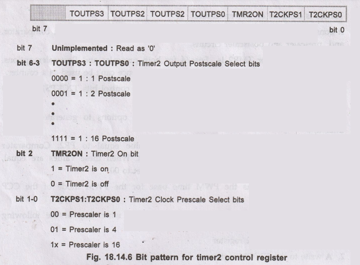
•
Timer2 can be shut-off by clearing control bit TMR2ON (T2CON register) to
minimize power consumption.
c.
Block Diagram
•
Fig. 18.14.7 shows the simplified block diagram of Timer 2.
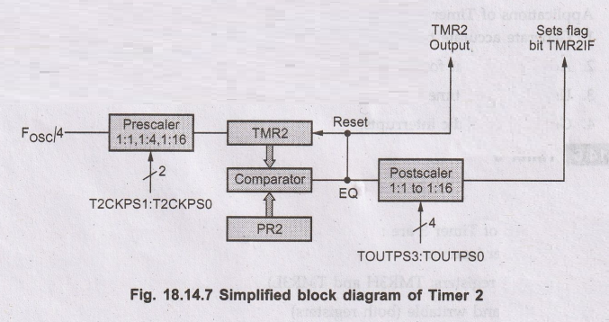
•
Timer2 is disabled on power-on-reset.
•
It consists of two 8-bit, readable/writable registers: TMR2 and PR2,
comparator, and prescaler and postscaler circuits.
•
The clock source for TMR2 is Fosc/4 for both prescaler and Postscaler options.
There is no external clock source for Timer2 and hence can't be used as a
counter.
•
The prescale option of 1:1, 1:4 or 1:16, selected by control bits
T2CKPS1:T2CKPS0 (T2CON register).
•
The 4-bit postscaler gives a 1:1 to 1:16 scaling options to generate a TMR2
interrupt.
•
TMR2 register increments from 00 to the value equal to PR2. Comparator compares
values from TMR2 and PR2 registers. When these values are equal, TMR2IF flag is
set in PIR1 register and TMR2 reset to 00.
•
Timer2 can be used as the PWM time base for the PWM mode of the CCP module.
•
The prescaler and postscaler counters are cleared when any of the following Occurs:
1.
A write to the TMR2 register
2.
A write to the T2CON register
3.
Any device Reset (Power-on Reset, MCLR Reset, Watchdog Timer Reset or Brown-out
Reset)
•
TMR2 is not cleared when T2CON is written.
d.
Applications
•
Applications of Timer 2 are:
1.
Generate accurate time delays by selecting the appropriate prescaler options.
2.
Acts as an input for SSP module to generate clock shift.
3.
Used as PWM time base for the PWM mode of the CCP module.
4.
Generate periodic interrupts.
6. Timer 3
a.
Features
The
features of Timer 3 are:
1.
16-bit timer/counter TUOT
2.
Two 8-bit registers: TMR3H and TMR3L)
3.
Readable and writable (both registers)
4.
Internal or external clock select
5.
Interrupt-on-overflow from FFFFh to 0000h
6.
Reset from CCP1/ECCP1 module trigger
b.
T3CON: Timer3 Control Register
•
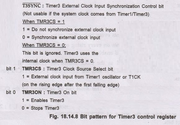
Fig. 18.14.8 shows the Timer3 Control register (T3CON). It is an 8-bit,
read/write register used to that controls all the aspects of Timer3.
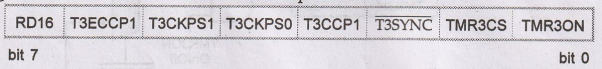
bit
7 RD16 : 16-bit Read/Write Mode Enable
bit
1
= Enables register read/write of Timer3 in one 16-bit operation
0
= Enables register read/write of Timer3 in two 8-bit operation
bit
6,3 T3ECCP1: T3CCP1 : Timer3 and Timer1 to CCP1/ECCP1 Enable
bits
1x
= Timer3 is the clock source for compare/capture CCP1 and ECCP1 modules
01
= Timer3 is the clock source for compare/capture of ECCP1
Timer1
is the clock source for compare/capture of CCP1
00=
Timer1 is the clock source for compare/capture of CCP1 and ECCP1 modules
bit
5-4 T3CKPS1 : T3CKPS0: Timer3 Input Clock Prescale Select
bits
11=
1:8 Prescale value
10
= 1:4 Prescale value
01
= 1: 2 Prescale value
00
= 1:1 Prescale value
c.
Block Diagram
•
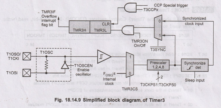
Fig. 18.14.9 shows the simplified block diagram of Timer3.
•
Timer3 can be enabled/ disabled by setting/clearing control bit, TMR3ON (T3CON
register).
•
The operating mode for the Timer3 is determined by the clock select bit, TMR3CS
(T3CON register). Timer3 can operate in one of these modes:
■
As a timer
■
As
a synchronous counter
■
As
an asynchronous counter
•
When TMR3CS = 0, Timer3 increments every instruction cycle.
•
When TMR3CS = 1, Timer3 increments on every rising edge of the Timer1 external
clock input or the Timer1 oscillator, if enabled.
•
The Timer1 oscillator may be used as the clock source for Timer3. When the
Timer1 oscillator is enabled (T1OSCEN is set), the T1OSI and T1OSO/T1CKI pins
become inputs.
•
Timer3 also has an internal "Reset input". This Reset can be generated
by the CCP module.
•
The prescaler circuit divides the signal frequency by prescale values of 1:1,
1: 2, 1: 4, 18 according to the status of T3CKPS1:T3CKPS0: Timer3 Input Clock
Prescale Select bits.
•
Here, TMR3IF flag bit is set when 16-bit timer value in TMR3 register pair
(TMR3H:TMR3L) increments from 0000h to FFFFh and rolls over to 0000h.
d.
Applications
•
Applications of Timer 3 are:
■
Generate accurate time delays by selecting the appropriate prescaler options.
■
Measure
frequency of an unknown signal.
■
Implement
Real Time Clock (RTC)
■
Generate
special event trigger in compare mode of CCP module.
7. Delay Calculations
•
Let's take an example. Suppose we have to generate a delay of 1 ms having 10
MHZ oscillator frequency of PIC18F458.
Calculate
timer input frequency
Given:
FOSC = 10 MHz. Let us take prescaler = 1 : 4
FTIMER
= FOSC / 4 × Prescaler ratio
=
10 / 4 × 1 / 4 = 625 kHz
Find
the period which will be taken by the timer to increment the count
Period
= 1 / FTIMER = 1/ 625 kHz = 1.6 μs
•
Therefore, after each 1.6 μs, the timer value will be incremented by 1.
Find
the count needed for a delay of 1 ms
Count
= 1 ms / 1.6μs = 625
•
Since this count is greater than 256 we need use 16 bit timer.
Calculate
value to be loaded in Timer register for a delay of 1 ms
•
The value to be loaded in 16-bit Timer register is calculated as: 65536- Count
= 65536 625 = 64911 = FD8FH
•
Load this hex value in the 16-bit timer register to produce desired delay.
Using
8-bit Timer
•
By selecting larger prescaler ratio we can generate same delay with 8-bit
counter. Let us select prescaler 1 : 64.
FTIMER
= FOSC / 4 × Prescaler ratio
=
10 / 4 × 1 / 64 = 39.0625 kHz
Find
the period which will be taken by the timer to increment the count
Period
= FTIMER = 1 / 39.0625 kHz = 25.6 µs
•
Therefore, after each 25.6, us the timer value will be incremented by 1.
Find
the count needed for a delay of 1 ms
Count
= Desired Delay / Timer Period = 1 ms / 25.6μs
=
39.0625≈ 39
•
Since this count is less than 256 we need use 8- bit timer.
•
The value to be loaded in 8-bit Timer register is calculated as: 256 - Count
256 - 39 = 217 D9H
•
Load this hex value in the 8-bit timer register to produce desired delay.
Review Questions
1. How many timers
are available in PIC18 microcontroller?
2. How many timers
are available in PIC18F458 microcontroller?
3. Lists control and
count registers for timers available in PIC18F458 microcontroller.
4. State various
clock sources available for timers in PIC18F458 microcontroller.
5. Describe
prescaling.
6. List the features
of Timer0.
7. Draw and explain
the bit pattern for Timer0 Control Register
8. Explain timer 0
mode of PIC18XX and its applications in detail.
9. Draw and explain
the simplified block diagram for Timer0 in 8-bit mode.
10. Draw and explain
the simplified block diagram for Timer0 in 16-bit mode.
11. List the
features of Timer1.
12. Draw and explain
the bit pattern for Timer1 Control Register.
13. Explain timer 1
mode of PIC18XX and its applications in detail.
14. Draw and explain
the simplified block diagram for Timer1.
15. List the
features of Timer2.
16. Draw and explain
the bit pattern for Timer2 Control Register.
17. Explain timer2
mode of PIC18XX and its applications in detail.
18. Draw and explain
the simplified block diagram for Timer2.
19. List the
features of Timer3.
20. Draw and explain
the bit pattern for Timer3 Control Register.
21. Explain timer3
mode of PIC18XX and its applications in detail.
22. Draw and explain
the simplified block diagram for Timer3.
23. Explain the delay calculations for timers in PIC18.
Microprocessors and Microcontrollers: Unit V: (b) Introduction to RISC Based Architecture : Tag: : Introduction to RISC Based Architecture - Timers