Electron Devices and Circuits: Unit III: (a) BJT Amplifiers
Transistor Hybrid Model
4 h-parameters and its benefits | BJT Amplifiers
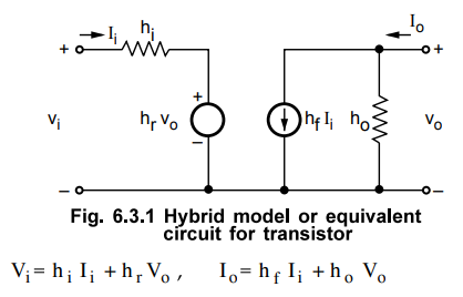
• In order to analyze transistorized amplifier circuit and calculate its input impedance, output impedance, current gain and voltage gain, it is necessary to replace transistor circuit with its h-parameter equivalent.
Transistor Hybrid Model
AU
: Dec.-13, May-15
•
In order to analyze transistorized amplifier circuit and calculate its input
impedance, output impedance, current gain and voltage gain, it is necessary to
replace transistor circuit with its h-parameter equivalent.
•
The h-parameter equivalent circuit can be drawn with the help of two equations,
as shown in Fig. 6.3.1.
1. Benefits of h-parameters
1.
Real numbers at audio frequencies.
2.
Easy to measure.
3.
Can be obtained from the transistor static characteristic curves.
4.
Convenient to use in circuit analysis and design.
5.
Most of the transistor manufacturers specify the h-parameters.
2. h-Parameter Model for the Common-Emitter Configuration
•
To see how we can derive a hybrid model for a transistor, let us consider the
common emitter configuration shown in Fig. 6.3.2. The variables Ib, Ic, Vb and
Vc represent total instantaneous currents and voltages.

Ib
= Input current
Ic
= Output current
Vbe
= Input voltage
Vce
= Output voltage
•
Fig. 6.3.3 shows the h-parameter equivalent circuit for the common emitter
configuration.
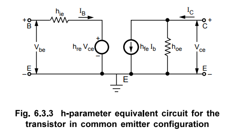
Fig.
6.3.3 h-parameter equivalent circuit for the transistor in common emitter
configuration
•
From the h-parameter equivalent circuit of the common emitter configuration we
can write,
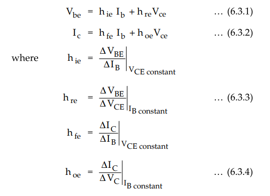
•
The quantities Δ VBE (Vbe), Δ VCE (Vce) Δ IB
(Ib) and Δ IC (Ic) represent the small change in base and
collector voltages and currents.
3. h-Parameters for all Three Configurations
•
For different configurations the relation between input parameters and output
parameters also differs. Therefore, one needs to define different set of
h-parameters for different configurations.
•
To designate the type of configuration subscript belongs to specified
configuration is added to the h-parameters. This is illustrated in Table 6.3.1.

•
The basic circuit of hybrid model is same for all the three configurations,
only parameters are different.
•
The Fig. 6.3.4 shows the transistor configurations and their hybrid models.

•
The circuits and equations in Fig. 6.3.4 are valid for either an n-p-n or p-n-p
transistor and are independent of the type of load or method of biasing.
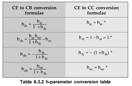
4. Relationship between h-Parameters Different Transistor
Configurations
•
Most of the times h-parameters are specified for common emitter configuration,
therefore, for analysis of common collector and common base configurations we
have to first convert given h-parameters for common emitter configuration into
the desired configuration by using conversion formulae given in Table 6.3.2.
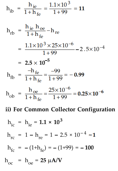
Ex. 6.3.1 The h-parameter for the transistor are hie= 1.1 k Ω, hfs = 99, hrs = 2.5 × 10⁻⁴ and hoe = 25 A|V. Find the h-parameters for common base and common collector configurations.
Sol.
: i) For Common Base Configuration
5. Determination of h-Parameters from CE Characteristics
•
Let us consider common emitter configuration. Its functional relationship can
be defined from equations 6.2.1 and 6.2.2 from section 6.2 as
Vbe
– f1 (Ib,Vce) ...(6.3.5)
Ic
= f2 (Ib,Vce) ...(6.3.6)
•
We have already seen the relationship between input and output voltages and
currents from the characteristic curves. The input characteristic curves give
the relationship between input voltage VBE and the input current IB for different
values of output voltage VCE
•
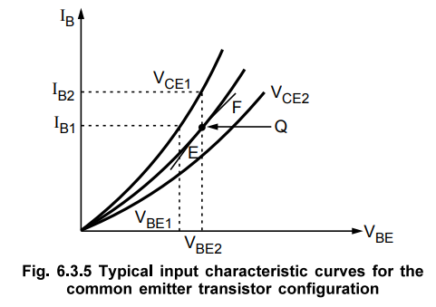
Fig. 6.3.5 shows typical input characteristic curves for the common emitter
transistor configuration.
Determination
of hie and hre from Input Characteristic Curves
Parameter
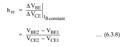
hie : From equation (6.3.3) we have,

•
The parameter hie can be obtained as the change in the base voltage,
VBE2 - VBE1, divided by the change in the base current, IB2
-IB1, for a constant collector voltage at the quiescent point, Q.
•
The slope of the line EF, drawn tangent to the input characteristic curve at
the point Q gives hie.
Parameter
hre : From equation (6.3.3) we have,
• A horizontal line on the input characteristics of Fig. 6.3.5 represents constant base current. The parameter hre can be obtained as the change in base voltage, VBE2 - VBE1, divided by the change in collector voltage, VCE2 - VCE1, for a constant base current IB, at the quiescent point Q.
•
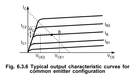
The output characteristic curves give the relationship between output current,
IC and output voltage, VCE for different values of input current IB. Fig. 6.3.6
shows typical output characteristic curves for the common emitter transistor
configuration.
Determination
of hie and hre from Ouput Characteristic Curves
•
From equation (6.3.4) we have, A

•
It is the ratio of change in collector current IC taken around the quiescent
point Q to the corresponding change in the base current IB, for constant value
of output voltage VCE at the Q-point.
Parameter
hoe :
•
From equation (6.3.4) we have,
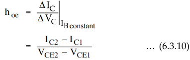
•
The parameter hoe can be obtained as the change in the collector
current, IC2 -IC1, divided by the change in the collector voltage, VCE2 - VCE1,
for a constant base current at the quiescent point Q. The slope of the line AB,
drawn tangent to the output characteristic curve at the point Q gives hoe. By
using similar procedure it is possible to obtain h-parameters for common base
and common collector configurations from the appropriate input and output
characteristic curves.
•
From the above discussion it can be noticed that h-parameters are always
calculated at quiescent operating point of the amplifier.
Review Questions
1. Define the four h-parameters.
2. Define the various h-parameters for a common emitter
transistor.
3. List the benefits of h-parameters.
4. Obtain the hybrid model of CE transistor and define the
hybrid parameters.
5. Draw the hybrid model of transistor in CE and CB configurations.
6. Explain, how h-parameter can be obtained from the transistor
characteristics.
Electron Devices and Circuits: Unit III: (a) BJT Amplifiers : Tag: : 4 h-parameters and its benefits | BJT Amplifiers - Transistor Hybrid Model
Related Topics
Related Subjects

Electron Devices and Circuits
EC3301 3rd Semester EEE Dept | 2021 Regulation | 3rd Semester EEE Dept 2021 Regulation