Electron Devices and Circuits: Unit I: PN Junction Devices
Transition Capacitance (CT)
PN Junction Diode
• As seen earlier, when a diode is reverse biased, reverse current flows due to minority carriers. Majority charged particles i.e. electrons in n-region and holes in p-region move away from the junction. This increases the width of the depletion region.
Transition Capacitance (CT)
AU
: Dec.-02, 03, 16, May-03, 06, 16
•
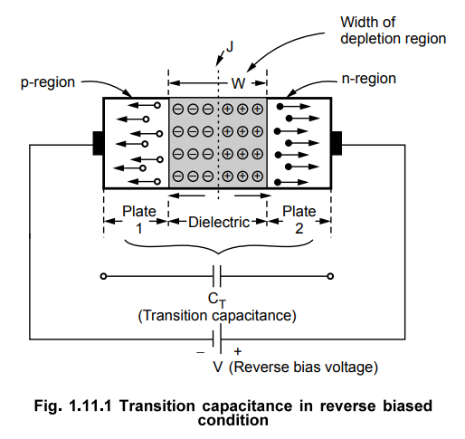
Consider a reverse biased p-n junction diode as shown in the Fig. 1.11.1.
condition
•
As seen earlier, when a diode is reverse biased, reverse current flows due to
minority carriers. Majority charged particles i.e. electrons in n-region and
holes in p-region move away from the junction. This increases the width of the
depletion region. The width of the depletion region increases as reverse bias
voltage increases. As the charged particles move away from the junction there
exists a change in charge with respect to the applied reverse voltage. So
change in charge dQ with respect to the change in voltage dV is nothing but a
capacitive effect. Such a capacitance which comes into the picture under
reverse biased condition is called transition capacitance, space-charge
capacitance, barrier capacitance or depletion layer capacitance and denoted as
C’T. The magnitude of CT is given by the equation,
CT
= dQ / dV ... (1.11.1)
•
This capacitance is very important as it is not constant but depends on the
magnitude of the reverse voltage.
•
If W is the width of the depletion region then transition capacitance is given
by,
CT
= ƐA / W
where
A = Area of cross-section of the junction
Ɛ
= Permittivity of the semiconductor
•
As the reverse biased applied to the diode increases,
the
width of the depletion region (W) increases. Thus the transition capacitance CT
decreases. In short, the capacitance can be controlled by the applied voltage.
The variation of CT with respect to the applied reverse bias voltage is shown
in the Fig. 1.11.2.
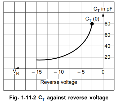
•
As reverse voltage is negative, graph is shown in the second quadrant. For a
particular diode shown, CT varies from 80 pF to less than 5 pF as VR changes
from 2 V to 15 V.
•
As the transition capacitance varies with the applied voltage, it can be used
as a voltage variable capacitance in many applications. In practice, special
type of diodes are manufactured which shows the transition capacitance property
more predominantly as compared to the normal diodes. Such diodes are called
varactor diodes, varicap, WC (voltage variable capacitance) or tuning diodes.
1. Derivation of Expression for Transition Capacitance
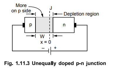
•
Consider the p-n junction whose p side is lightly doped than n side.
•
Such an unequally doped p-n junction is shown in the Fig. 1.11.3, which is
reverse biased.
•
The depletion region penetrates more on lightly doped side hence its width is
more on p side.
•
Practically it can be assumed that concentration of impurity on both sides is
such that the entire depletion region is on p side only.
•
Let NA = Concentration of acceptor impurity on p side
•
The relation between potential V and charge density NA is given by
Poisson's equation as,
d2V
/ dx2 = qNA / Ɛ
...x
= Distance measured from junction
Ɛ
= Ɛ0 Ɛr = Permittivity of semiconductor
where
Ɛ0
= 8.854 × 10⁻¹² F/m
and Ɛr = 16 for Ge and 12 for Si
Integrating
above equation with respect x,
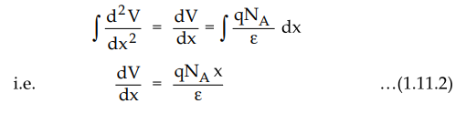
•
But dV/dx is the electric field E over the region x = 0 to x = W over which
depletion region exists.
E
= qNAx / Ɛ ... q = Charge on each electron ...(1.11.3)
Integrating
equation (1.11.2)
At
x = W, V = VB = Barrier potential which is the difference between junction potential
Vj and applied reverse bias V
i.e. VB = VJ - V ...(1.11.5)
•
V must be taken as negative as reverse biased. Hence as V becomes more negative,
VB = VJ - (- V) = VJ + V increases.
•
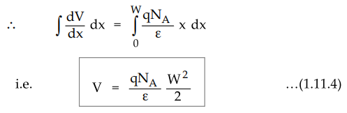
Using in equation (1.11.4),
VB
= qNA / Ɛ W2/2 ,
i.e. W ∝ √VB ...(1.11.6)
The
width of depletion region increases as applied reverse bias voltage increases
•
If A is the area of cross-section of junction, W is the width then net charge Q
in the distance W is,
Q
= NA × Volume × q
=
NA AWq ...(1.11.7)
•
Differentiating equation (1.11.4) with respect to V,
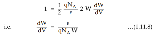
'
Differentiating equation (1.11.7) with respect to V,
dQ
/ dV = NA A dw/dv q … (1.11.9)
'
Using equation (1.11.8) in (1.11.9) and dQ/dV = CT.
CT
= ƐA / W = Transition capacitance ... (1.11.10)
Thus
CT ∝ 1/W
and hence as reverse bias increases, the width of the depletion region W
increases and hence transition capacitance CT decreases.
Review Questions
1. Discuss about the capacitance effect of a reverse biased p-n
junction diode. What is its importance ?
AU : Dec.-02, 03, Hay-03, 06, 16, Harks 8
2. Derive the expression of the Space charge or Transition
capacitance of PN diode under reverse bias with a neat diagram.
Electron Devices and Circuits: Unit I: PN Junction Devices : Tag: : PN Junction Diode - Transition Capacitance (CT)
Related Topics
Related Subjects

Electron Devices and Circuits
EC3301 3rd Semester EEE Dept | 2021 Regulation | 3rd Semester EEE Dept 2021 Regulation