Electron Devices and Circuits: Unit I: PN Junction Devices
Two Marks Questions with Answers
PN Junction Devices | Electron Devices and Circuits
Electron Devices and Circuits: Unit I: (b) PN Junction Devices : Two Marks Questions with Answers
Two Marks Questions with Answers
Q.1
What is diffusion current in PN junction diode?
AU
: Dec.-02, 06, 09. 13. May-03, 10
Ans.
:
When a semiconductor is nonuniformly doped, then there exists concentration
gradient. On one side there is high carrier concentration while on the other
there is low carrier concentration. Due to this, charges start moving from
higher to lower concentration area. This process is called diffusion. When the
charges move due to diffusion, the current gets established in a semiconductor
which is called a diffusion current.
Q.2
What is LED ? Which material is used for LED ?
AU
: Dec.-09
Ans.
:
LED is a light emitting diode. When forward biased this diode emits light of
different colours depending on the material used.

Q.3
What is peak inverse voltage ?
AU
: May-06, Dec.-lO
Ans.
:
In reverse biased, opposite polarity voltage appears across diode. The maximum
reverse voltage which diode can withstand without breakdown is called peak
inverse voltage.
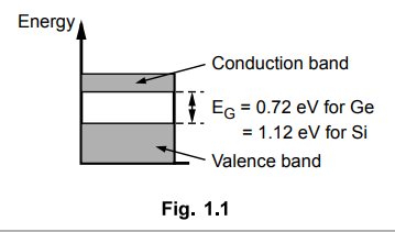
Q.4
Draw the energy band structure of Silicon and Germanium at room temperature
indicating the energy gap (Ec) value in eV.
Ans.
:
The energy band structure is shown in the Fig. 1.1.
Q.
5 What is meant by zener breakdown?
Ans.
:
When a p-n junction is heavily doped the depletion region is very narrow. So
under reverse bias conditions, the electric field across the depletion layer is
very intense. Electric field is voltage per distance and due to narrow
depletion region and high reverse voltage, it is intense. Such an intense field
is enough to pull the electrons out of the valence bands of the stable atoms.
Such a creation of free electrons is called zener effect. These minority
carriers constitute very large current to cause the breakdown and the mechanism
is called zener breakdown.
Q.6
Compare the Silicon and Germanium diodes with respect to cut-in voltage and
reverse saturation current.

Q.7
Define barrier pptential at the junction
Ans.
:
Due to immobile positive charges on n side and negative charges on p side,
there exists an electric field across the unbiased p-n junction. This creates
potential difference across the junction which is called a barrier potential.
Thus the voltage existing across the depletion region or barrier is called a
barrier potential.
Q.8
Give the diode current equation.
Ans.
:
The diode current equation is,
I
= I0[eV/ηVT -1] A
where I0 = Reverse saturation
current in amperes
V
= Applied voltage, VT = Voltage equivalent of temperature in volts
η
= 1 for germanium diode and 2 for silicon diode
Q.9
Define knee voltage or a cut-in voltage of a diode.
AU
: Hay-06, 07, Dec.-lO
Ans.
:
When diode is forward biased, some voltage is necessary to overcome barrier
potential, to make diode conduct. This is called its cut-in voltage. The
minimum voltage at which the diode starts conducting and current starts
increasing exponentially is called cut-in voltage, offset voltage, break-point
voltage, threshold voltage or knee voltage. It is denoted as V, and its, value
is 0.2 V for Germanium while 0.6 V for Silicon. Below this voltage, the diode
current is very very small and practically considered to be zero.
Q.10
What is meant by depletion region ?
AU
: Dec.-07, Hay-09
Ans.
:
In a P-N junction, the diffusion of holes and electrons start initially. Near
the junction, holes recombine in n-region to from immobile positive ions.
Similarly electrons recombine in p-region to form immobile negative ions. With
sufficient accumulation of such immobile ions on both sides, the diffusion
stops. So near the junction, there exists a region in which immobile positive
and negative charges reside while mobile charge carriers in this region get
completely depleted. This region is called depletion region.
Q.11
Define the transition capacitance of a diode.
AU
: Hay-08, Dec.-07,14
Ans.
:
A capacitance existing at the P-N junction when the diode is reverse biased
where the two regions act as the plates while the depletion region acts as
dielectric is called a transition capacitance of a diode.
Q.12
Write a short note on applications of diode.
AU
: Dec.-07, Hay-16
Ans.
:
The main application of a diode is rectifier circuits which converts a.c. to
d.c. The various diode rectifier circuits are half wave rectifier, full wave
rectifier and bridge rectifier circuits. The diodes are used in clipping
circuits. The diode is also used in the clamper circuits in which a necessary
d.c. level is added to the waveform. The diodes are effectively used in voltage
multiplier circuits where the output is integer multiple of the input voltage. The diodes are also used in
multivibrator circuits. With the operational amplifiers, the diodes are used in
variety of applications such as multipliers, log amplifiers, antilog
amplifiers, oscillator amplitude stabilization circuits, precision rectifiers
etc. The varactor diodes are used in tunned circuits, FM modulators, automatic
frequency control devices etc. The LEDs are used for the displays, various
optical devices, on-off indicator etc. While the photo diodes are used in alarm
systems, counter operations etc.
Q.13
Draw the VJ characteristics of a PN junction diode. (Refer section 1.8)
Q.14
Why a series resistor is necessary when a diode is forward biased ?
Ans.
: For
limiting the forward current which increases exponentially with voltage.
Q.15
List any four applications of light emitting diode.
AU
: Hay-08
Ans.
:
1.
All kinds of displays used in watches and calculators.
2.
In the optical devices such as opto-couplers.
3.
As on-off indicator in various electronic circuits.
4.
In remote controls and burgler alarms.
Q.16
What is meant by breakdown voltage in PN junction diode ?
Ans.
:
In reverse biased condition, as reverse voltage increases the reverse current
is almost constant upto certain value of reverse voltage. At some reverse
voltage, the diode breaks down and large reverse current flows through it. The
voltage at which the diode breakdown occurs is called reverse breakdown
voltage.
Q.17
State the expression for the dynamic resistance of a diode.
Ans.
:
The dynamic resistance of a diode is given by,
r
= ηVT / I0 eV/ηVT
where
I0 = Reverse saturation current in amperes,
V
= Applied voltage,
VT
= Voltage equivalent of temperature in volts,
η
= 1 for Ge diode and 2 for Si diode
Q.18
List the disadvantages of half wave rectifier circuit.
Ans.
:
1.
High ripple factor.
2.
Efficiency is low.
3.
Low transformer utilisation factor.
4.
Can cause d.c. saturation of the transformer core as d.c. current flows through
the secondary of the transformer.
5.
Cost is more.
Q.19
What are the advantages of bridge rectifier over its center tapped counter part
?
(Refer
section 1.17.5)
Q.20
Compare the performance of half wave rectifier and full wave rectifier.
(Refer
section 1.16.17)
Q.21
Compare bridge rectifier with two diode full wave rectifier. (Refer section
1.17.8)
Q.22
Draw the full wave bridge rectifier circuit. (Refer section 1.17)
Q.23
Draw the block schematic of regulated power supply. (Refer section 1.23)
Q.24
Briefly explain how zener diode can be used as a regulator.
(Refer
section 1.24)
Q.25
Compare zener breakdown and avalanche breakdown in zener diode.
(Refer
section 1.22.3.3)
Q.26
Compare zener diode with conventional diode. (Refer section 1.22.4)
Q.27
What is meant by dynamic resistance of a diode ?
Ans.
:
The resistance offered by the p-n junction diode under a.c. conditions is
called dynamic resistance of a diode. It is the ratio of incremental change in
voltage applied to the corresponding change in the current of the diode. In
forward biased condition it is the slope of the forward characteristics of a diode.
Q.28
What is hole and electron in p-n junction diode ?
AU
: May-11
Ans.
:
Holes and electrons are the two charge carriers in p-n junction diode.
Electrons are negatively charged while holes are positively charged particles.
The holes are imaginary and considered due to absence of electron. Both the
charge carriers are responsible for the flow of current through the diode.
Q.29
Differentiate drift and diffusion current.
Ans.
:
When a voltage is applied to a material, the free electrons move towards the
positive of the battery. While moving they collide with the adjacent atoms and
keep changing their directions randomly. Still they keep drifting towards the
positive of the battery. This is called drifting of charge carriers and the
current due to such drifting of charge carriers is called drift current.
In
case of diffusion current, the external voltage is not required. Due to
nonuniform doping of the material, a concentration gradient is created across
the material due to which the charge carriers move from higher to lower
concentration area. This is called diffusion and the corresponding current is
called diffusion current.
Q.30
What is p-n junction diode ?
Ans.
:
The two materials namely p-type and n-type are chemically combined with a
special fabrication technique to form p-n junction. There are two electrodes
each from p-type and n-type materials and due to these two electrodes
(di+electrode), the device is called a diode. It conducts only in one
direction.
Q.31
Mention the applications of zener diode.
AU
: Dec.-16
Ans.
:
1.
As a voltage regulating element in regulators
2.
In various protection circuits
3.
In clipping circuits
Q.32
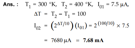
A silicon diode has a saturation current of 7.5 µA at room temperature 300 °K.
Calculate
the saturation current at 400 °K.
AU
: Hay-10, Dec.-16
Ans.
:
Q.33
What is the value of VT (Volt equivalent of temperature) at a temperature of
300 °K ?
AU
: Dec.-04
Ans.
:
VT = kT = 8.62 × 10-5 × (300) = 0.02586 V
34.
Derive the ripple factor of FWR.
AU
: Dec.-05, 08, Hay-06, 07
Ans.
:
The ripple factor is given by,

Q.35
Define transformer utilization factor. State its value for half wave rectifier.
Ans.
:
The T.U.F. is defined as the ratio of d.c. power delivered to the load to the
a.c. power rating of the transformer.
T.U.F.
= D. C. power delivered to the load / A. C. power rating of the transformer
Its
value for half wave rectifier is 0.287.
Q.36
Define ripple factor.
Ans.
:
Mathematically, ripple factor is defined as the ratio of R.M.S. value of the
a.c. component in the output to the average or d.c. component present in the
output.
Ripple
factor
ɤ
= R.M.S. value of a.c. component of output / Average or d. c. component of
output
=
Iac / IDC
Q.37
Derive the ripple factor of HWR.
AU
: May-06, 07, Dec.-08
Ans.
:
For a half wave circuit, IRMS = 1m / 2

Q.38
Define voltage regulation.
Ans.
:
The voltage regulation is the factor which tells us about the change in the
d.c. output voltage as load changes from no load to full load condition.
If
(Vdc )NL = D.C. voltage on no load
(Vdc
)FL = D.C. voltage on full load
then
voltage regulation is defined as,
Voltage
regulation = (Vdc )NL - (Vdc )FL / (Vdc
)FL
Q.39
Compare the transformer utility factors of half wave rectifier and bridge
rectifier and reason out the better one.
Ans.
:
For half wave rectifier, T.U.F. is 0.287 while for the bridge rectifier it is
0.812. This is because the entire secondary of the transformer carries the
current all the time and hence transformer is utilized in better way.
Q.
40 The theoretical maximaum conversion efficiency of half wave rectifter is
……..
Ans
:
40.6 %
Q.
41 The theoretical maximaum conversion efficiency of half wave rectifter is
Ans
:
81.2 %
Q.
42 What is voltage regulator?
Ans
:
The voltage regulator is a circuit which keeps the output voltage constant
inspite of changes in load current or input voltage.
Q.
43 What is temperature is coefficient of
a Zener diode?
Ans
: The percentage change in the Zener voltage VZ for every oC
change in temperature is called temperature coefficient of a Zener diode. It is
denoted as TC and expressed as % / °C.
Mathematically
it can be defined as,
TC
= ΔVZ / VZ (T1
–T0 ) × [l00%] %/°C
where
T1 is the final temperature of junction while T0 is
generally 25 °C at which nominal Zener voltage Vz is specified.
Q.44
What are the limitations of using Zener diode regulator ?
Ans.
:
1.
The maximum load current that can be supplied is limited to [IZmax –
IZmin].
2.
A large amount of power is wasted in the zener diode and the series resistance
R, in comparison with the load power.
3.
The stability factor and the output resistance are not very low, as desired for
a regulator circuit.
Q.45
What is a PN junction ? How is it formed ?
AU
: May-12
Ans.
:
The two types of materials namely p-type and n-type are chemically combined
with a special fabrication technique to form a junction called p-n junction.
The n-type material has large number of free electrons while p-type material
has large number of holes. Due to diffusion the charge carriers cross the
junction and immobile ions are formed on either side of p-n junction, forming a
region which is free from mobile charge carriers. This region is called
depletion region of p-n junction.
Q.46
What is LED ? Draw it's symbol.
Ans.
:
LED is a light emitting diode which emits light when forward biased. The colour
of light depends on the material used. The symbol is shown in the Fig. 1.2.

Q.
47 Calculate the speed of electron when it jails by a potential of 300 k volts.
AU
: Dec.-12
Ans
:
The speed of electron is given by,
v
= √2qV / m m/s
where
q = Charge on electron = 1.6 × l0-19 C
m
= Mass of electron = 9.107 × l0-31 kg
V
= Potential applied
v
= √2 × l.6 × l0-19 × 300 × l03 / 9.107 ×10-31
=
324.8 × 10⁶ m/s
Q.48
Define static and dynamic resistance of a PN diode.
AU
: May-13, 16
Ans.
:
For dynamic resistance, refer Q.27.
The
static resistance is the resistance offered by a diode under d.c. conditions.
At any point on the characteristics, static resistance is defined as the ratio
of the d.c. voltage applied to the p-n junction to the d.c. current flowing
through the p-n junction corresponding to that point.
Q.49
What is a rectifier ? List its types.
AU
: Dec.-13,14, Hay-15
Ans.
:
A rectifier is a device which converts a.c. voltage to pulsating d.c. voltage,
using one or more p-n junction diodes. The various types of rectifiers are,
i)
Half wave ii) Full wave and iii) Bridge type
Q.50
Compare rectifier and regulator.
Ans.
:
Rectifier
1.
Converts a.c. into pulsating d.c.
2.
The output contain ripples.
3.
Output changes with load current, input voltage and temperature.
4.
The diodes are commonly used.
5.
Not provided with protection circuits.
Regulator
1.
Converts pulsating d.c. into constant d.c.
2.
The output is ripple free.
3.
Output voltage does not change with load, input voltage and temperature.
4.
Transistors, op-amps, zener diodes are used.
5.
Provided with various types of protection circuits.
Q.51
What is diffusion capacitance ?
AU
: May-15, Dec.-14
Ans.
:
In forward biased condition, the width of the depletion region decreases and
holes from p side get diffused in n side while electrons from n side move into
the p side. As the applied voltage increases, concentration of injected charged
particles increases. This rate of change of the injected charge with applied
voltage is defined as a capacitance called diffusion capacitance.
Q.52
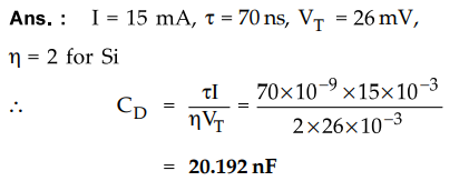
Calculate the diffusion capacitance for a silicon diode with a 15 mA forward
current, if the charge carrier transit time is 70 nsec.
Ans.
:
Q.53
Mention some of the applications of laser diode.
AU
: May-17
Ans.
:
The applications of laser diode are optical discs, CD players, laser printers,
fiber and broadband communication, aerospace and defence applications.
Q.54
Find the current I in the following circuit.

Ans.
: The
diode Dj is forward biased while D2 is reverse biased. Hence the equivalent
circuit is as shown in the Fig. 1.3 (a).
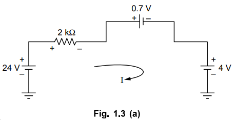
Applying
KVL,
-
2 × 10⁻³ I – 0.7 – 4 + 24 = 0
I
= 9.6 mA
Q.55
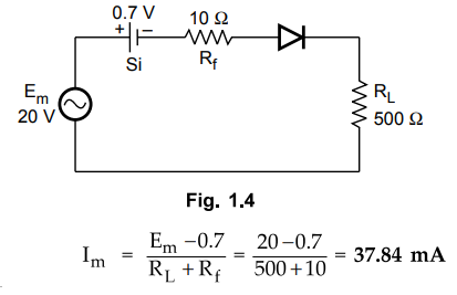
An a.c. voltage of peak value 20 V is connected in series with a silicon diode
and load resistance of 500 Q. If the forward resistance of diode is 10 Q find
the peak current through the diode.
AU
: Dec.-18
Ans.
:
The circuit with diode model is shown in the Fig. 1.4
Electron Devices and Circuits: Unit I: PN Junction Devices : Tag: : PN Junction Devices | Electron Devices and Circuits - Two Marks Questions with Answers
Related Topics
Related Subjects

Electron Devices and Circuits
EC3301 3rd Semester EEE Dept | 2021 Regulation | 3rd Semester EEE Dept 2021 Regulation