Electron Devices and Circuits: Unit II: (a) Bipolar Junction Transistors (BJT)
Two Marks Questions with Answers
Bipolar Junction Transistors (BJT) | Electron Devices and Circuits
Electron Devices and Circuits: Unit II: (a) Bipolar Junction Transistors (BJT) : Two Marks Questions with Answers
Two Marks Questions with Answers
Q.1
What is transistor ?
Ans.
:
Transistor is a three terminal device : Base, emitter and collector, can be
operated in three configurations common base, common emitter and common
collector. According to configuration it can be used for voltage as well as
current amplification.
Q.2
What are the terminals present in a transistor ?
Ans.
:
Three terminals : emitter, base, collector.
Q.3
State the two types of transistors.
Ans. : There are two types of
transistors : Unipolar junction transistor and Bipolar junction transistor.
Q.4
Why transistor is also called bipolar junction transistor ?
Ans.
:
The current conduction in bipolar transistor is because of both the types of
charge carriers, holes and electrons. Hence this is called Bipolar junction
transistor.
Q.5
Why transistor called a current controlled device ?
Ans.
:
In BJT output current is controlled by input current and hence it is a current
controlled device.
Q.6
Mention the types of BJT.
Ans.
:
The types of BJT are :
1.
n-p-n type 2. p-n-p type
Q.7
State the two junctions in the transistor.
Ans.
:
A transistor has two p-n junctions. One junction is between the emitter and the
base and is called the emitter base junction or simply the emitter junction JE.
The other junction is between the base and the collector and is called
collector-base junction or simply collector junction JC.
Q.8
What is doping ?
Ans.
:
The process by which impurities are added to a pure semiconductor is called
doping.
Q.9
Explain about the doping in transistor.
Ans.
:
The base region is very thin and lightly doped. The emitter and collector are
heavily doped. But the doping level in emitter is slightly greater than that of
collector.
Q.10
State the basic currents of the transistor.
Ans.
:
The basic currents of the transistor are : base current, collector current and
emitter current. They are related by equation IE = IB + IC.
Q.11
Define ɑdc and βdc
Ans.
: ɑdc is the fraction of IE
that crosses over from emitter to the collector region. βdc
is defined as the ratio of the collector current to the base current.
Q.12
Give the relation between _dc and pdc.
Ans.
:
β = ɑ / 1 - ɑ and ɑ = β / 1 + β
Q.13
What is the characteristics of a transistor ?
Ans.
:
Input characteristics : It is the relationship plotted graphically
between input voltage and input current while keeping output voltage as
constant.
Output
characteristics : It is the relationship plotted
graphically between the output voltage and output current while keeping input
current as constant.
Q.14
State the three operating regions of transistor.
Ans.
:
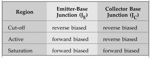
The three operating regions of transistor are : Active, cut-off and saturation.
Q.15
State the relation between operating region and biasing of transistor
junctions.
Ans.
:
The table gives the relation between operating region and biasing of transistor
junctions.
Q.16
When does a transistor act as a switch ?
Ans.
:
The transistor acts as a switch when it is operated at either cutoff region or
saturation region.
Q.17
What is early effect ?
Ans.
:
When reverse bias voltage VCB increases, the width of depletion region also
increases, which reduces the electrical base width. This effect is called as
Tiarly Effect' or 'Base width modulation'.
Q.18
What is emitter follower ?
Ans.
:
The common collector transistor amplifier is also called emitter follower.
Q.19
Define current amplification factor.
Ans.
:
It is defined as the ratio of change in output current to the change in input
current at constant.
Q.
20 Sketch typical common base output characteristics of a p-n-p transistor.
(Refer
section 2.8.1.3)
Q.
21 Will a transistor result if two diodes are connected back to back ?
(Refer
section 2.2)
Q.
22 State early effect. (Refer section 2.8.1.4)
AU
: May-02
Q.
23 Draw the output characteristics of n-p-n transistor in common emitter
configuration and mark the important regions of operation in it.
(Refer
section 2.8.2.3)
Q.
24. Define the h,e and hfe for a common emitter transistor configuration.
(Refer section 2.9)
AU
: May-04
Q.
25 What is early effect ? What are the consequences of it ?
(Refer
section 2.8.1.4)
Q.
26 When a transistor is used as a switch, in which regions of output
characteristics it is operated ?
(Refer
section 2.11)
Q.
27 Write the relation between Ia p, fB and ICB0 in a BJT. (Refer section 2.8)
Q.
28 Define _ and p of a transistor.
(Refer
section 2.6)
Q.
29 In a bipolar transistor, which region is wider and which is thinner ? Why ?
(Refer section 2.1)
AU
: May-06
Q.30
Which of the BJT configuration is suitable for impedance matching applications
? Why ? AU : Dec.-07
(Refer
section 2.8.4)
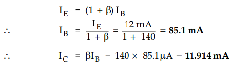
Q.
31 For a npn transistor Ig = 12 mA and p = 140. Determine the value of IB and
IQ.
AU
: May-08
Ans
.:
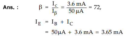
Q.32
Determine p and Ig for a transistor if lg = 50 pA 3.6 mA.
Ans.
:
Q.33
In bipolar junction transistors, mention the heavily doped and lightly doped
regions.
AU
: May-09
(Refer
section 2.2)
Q.34
Mention the biasing conditions of emitter base junction and collector base
junction in active region and cut-off region. (Refer section 2.2.2)
AU
: May-09
Q.
35 Why is collector region wider than emitter region in BJT ? (Refer section
2.4)
Q.36
In a BJT, the emitter current is 12 mA and the emitter current is 1.02 times
the collector current. Find the base current. (Refer example 2.3.1)
AU
: Dec.-09
Q.37
Draw the input and output characteristics of a transistor in CE configuration
and mark the cutoff, saturation and active regions.
(Refer
section 2.8.2)
AU
: May-10
Q.38
Name the operating modes of a transistor.
AU
: Dec.-lO
1.
Cut-off 2. Active 3. Saturation.
Q.39
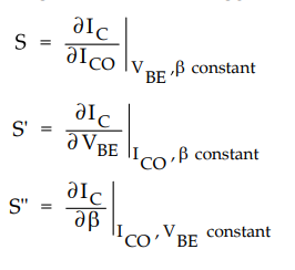
What is stability factor ? AU : May-11
Ans.
:
The stability factor is a measure of variation in IC (collector
current) due to change in ICO, VBE and β. It is defined
as three partial derivatives of I c with respect to I co VBE rnd β.
Q.40
What is the relation between Is,Ig and IQ in CB configuration ?
Ans.
: IE = IB + IC
Q.41
Among CE, CB and CC configurations, which one is the most popular ? Why ?
(Refer
section 2.8.5)
Q.42
Calculate β of a transistor when ɑ = 0.98
Ans
: β
= ɑ / 1 - ɑ = 0.98 / 1- 0.98 = 49
Q.43
List out the various biasing circuits.
AU
: ECE : Dec.-07, 10
Ans.
:
The various biasing circuits are :
1)
Fixed bias circuit
2)
Emitter bias circuit
3)
Voltage divider bias circuit
4)
Collector to base bias circuit.
Q.44
What is "thermal runaway" in transistors ?
AU
: ECE : Dec.-08
Ans.
:
The increase in the collector current increases the power dissipated at the
collector junction. This, in turn further increases the temperature of the
junction and hence increase in the collector current. The process is cumulative
and it is referred to as self heating. The excess heat produced at the
collector base junction may even bum and destroy the transistor. This situation
is called 'thermal runaway7 of the transistor.
Q.45
Draw the fixed bias and self bias circuit. (Refer sections 2.5 and 2.8.4)
AU
; ECE : May-06, 07, 08
Q.46
Why biasing is necessary in BJT amplifiers? (Refer section 2.5)
Q.47
Draw the fixed bias single stage transistor circuit. (Refer section Fig. 2.8.1)
AU
: ECE : May-04, 09
Q.48
What are the operating modes of BJT with reference to junction biasing ?
(Refer
section 2.3.2)
Q.49
What is meant by biasing ?
(Refer
section 2.5)
Q.50
Why collector region of a transistor is larger in area than emitter region ?
(Refer section 2.2)
AU
: May-12
Q.
51 Draw the neat circuit configuration of CB. (Refer section 2.4)
Q.
52 Draw the neat circuit configuration of CE.
(Refer
section 2.4)
Q.
53 Draw the neat circuit configuration of CC.
(Refer
section 2.4)
Q.
54 What is the advantage of using emitter resistance in the context of
biasing ? (Refer section 2.8)
AU
: Dec.-04
Q.
55 What is bias compensation using thermistor ?
(Refer
section 2.9)
Draw
a circuit that minimizes change in VBE due to temperature variation.
(Refer
section 2.9)
Q.
56 How can collector current be stabilized with respect to Ico variations ?
(Refer
section 2.9)
Q.
57 Why is temperature compensation required ?
(Refer
section 2.9)
Q.
58 Give the biasing arrangement for an NPN transistor to operate in the active
region.
(Refer
section 2.3)
Q.
59 Mention the biasing conditions of emitter base junction and collector base
junction in active region and cut-off region. (Refer section 2.3)
AU
: May-09
Q.
60 What are the types of transistor biasing ?
(Refer
section 2.8)
Q.
61 Draw the self bias circuit. (Refer section 2.8)
AU
: May-06, Dec.-08
Q.
62 Draw the single stage self-biased circuit using pnp transistor. (Refer
section 2.8)
Q.
63 Compare the characteristics of CE, CB and CC amplifiers. (Refer section
2.4.4)
Q.
64 Compare the performances of CE and CC configuration. [Section 2.4.4]
Electron Devices and Circuits: Unit II: (a) Bipolar Junction Transistors (BJT) : Tag: : Bipolar Junction Transistors (BJT) | Electron Devices and Circuits - Two Marks Questions with Answers
Related Topics
Related Subjects

Electron Devices and Circuits
EC3301 3rd Semester EEE Dept | 2021 Regulation | 3rd Semester EEE Dept 2021 Regulation