Electron Devices and Circuits: Unit II: (d) UJT Thyristor and IGBT
Two Marks Questions with Answers
UJT Thyristor and IGBT | Electron Devices and Circuits
Electron Devices and Circuits: Unit II: (d) UJT Thyristor and IGBT : Two Marks Questions with Answers
Two Marks Questions with Answers
Q.1
What is SCR ? Explain its construction in brief.
Ans.
:
SCR is a silicon controlled rectifier.
The
SCR is a four layer p-n-p-n device where p and n layers are alternately
arranged. The outer layers are heavily doped. There are three p-n junctions
called Ji J2 and J3. The outer p layer is called anode while outer n layer is
called cathode. Middle p layer is called gate. The three terminals are taken
out respectively from these three layers.
Q.2
Draw the characteristics of SCR.
(Refer
section 5.2.4)
Q.3
State any four specifications of SCR.
Ans.
: 1. Forward Breakover Voltage (VBO)
: It
is the voltage above which the SCR enters the conduction region ('ON'
state). The forward breakdown voltage is dependent on the gate bias.
2.
Holding Current (IH) : It is that value of
current below which the SCR switches from the conduction state (ON state) to
the forward blocking state.
3.
Latching Current (IL) : This is the minimum
current flowing from anode to cathode when SCR goes from OFF to ON state and
remains in ON state even after gate bias is removed. It is greater than, but
very close to holding current.
4.
Reverse Breakdown Voltage (VBR) : It is the reverse
voltage (Anode-negative and cathode-positive) above which the reverse breakdown
occurs, breaking J1 and J3 junctions. When the SCR is reversed biased, the
thickness of the J2 depletion layer during the forward bias condition is
greater than the total thickness of the two depletion layers at J1 and J3. Therefore,
the forward breakover voltage VfiO is greater than the reverse breakover
voltage VBR.
Q.4
State the applications of SCR.
Ans.
:
1.
Controlled rectifiers.
2.
A.C. voltage stabilizers.
3.
D.C. to D.C. converters called choppers.
4.
D.C. to A.C. converters called inverters.
5.
Dimmerstats to control light intensity.
6.
For speed control schemes of d.c. and a.c. motors called drives.
Q.5
Draw the equivalent circuit of UJT.
(Refer
section 5.1.2)
Q.6
What is interbase resistance of UJT ?
Ans.
:
When the emitter diode is not conducting then the resistance between the two
bases B1 and B2 is called interbase resistance denoted as
RBB.
RBB
= RB1 + RB2
Its
value ranges between 4 kΩ and 12 kΩ.
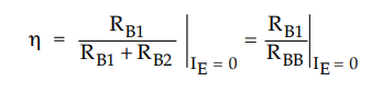
Q.7 Define intrinsic stand off ratio for UJT. AU:
May-12, 17
Ans. For UJT intrinsic stand off ratio is defined as
Q.8 Draw the characteristics of UJT.
(Refer section 5.1.5)
Q.9 State the applications of UJT.
Ans.
1.
Triggering of other devices like SCR.
2.
In a sawtooth waveform generator.
3.
In a relaxation oscillator.
4.
In timing circuits.
5.
In automobile ignition circuits.
Q.10
Draw the diac characteristics.
(Refer
section 5.4.3)
Q.11
State the applications of diac.
Ans.
:
1.
Triggering of triac
2.
Motor speed control
3.
Temperature control
4.
Light dimming circuit
5.
In air conditioning and other domestic applications.
Q.12
Draw the characteristics of triac.
(Refer
section 5.5.2)
Q.13
State the applications of triac.
Ans.
:
1.
Static d.c. switching of applications.
2.
In a three position static switch.
3.
A.C. power flashers.
4.
Heater or temperature controllers.
5.
As a triggering device for SCRs.
6.
Light dimmer circuits.
Q.14
Compare SCR and triac.
Ans.
:

Q.15
State the merits of IGBT.
(Refer
section 5.6.5.1)
Q.16
State the demerits of IGBT.
(Refer
section 5.6.5.2)
Q.17
State the applications of IGBT.
(Refer
section 5.6.5.3)
Q.18
What is a thyristor? Mention two of them.
Ans
:
AU:
May-15 Ans. A thyristor is a semiconductor device whose switching action
depends on internal regenerative feedback. Unlike BJTS and FETs, a thyristor
can be operated only as a switch. A thyristor can be two terminal, three
terminal or four terminal, unidirectional or bidirectional device.
The
two thyristors are silicon controlled rectifier (SCR) and Triac.
Q.19
Show how an SCR can be triggered on by the application of a pulse to the gate
terminal.
AU:
Dec.-15
Ans.
:
When the pulse is applied to the gate terminal then the electrons from n-type
cathode which are majority in number, cross the junction J 3 to reach to
positive of battery. While holes from p type move towards the negative of
battery, constituting gate current.
This
current increases the anode current as some of the electrons cross junction J2.
As anode current increases, more electrons cross the junction J2 and the anode
current further increases.
Due
to regenerative action, within short time, the junction J2 breaks and SCR gets
triggered. This is shown in the Fig. 5.7.1.

Q.20
Draw the symbol of the following devices, a) PN diode b) Zener diode c) LED d)
UJT
Ans.
:

Q.21
Draw the two transistor equivalent circuit of SCR.
Ans.
:
Refer Fig. 5.3.8 of section 5.3.3]
Q.22
Draw the structure of UJT.
Ans.
:
Refer Fig. 5.1.1 of section 5.1.1.
Electron Devices and Circuits: Unit II: (d) UJT Thyristor and IGBT : Tag: : UJT Thyristor and IGBT | Electron Devices and Circuits - Two Marks Questions with Answers
Related Topics
Related Subjects

Electron Devices and Circuits
EC3301 3rd Semester EEE Dept | 2021 Regulation | 3rd Semester EEE Dept 2021 Regulation