Electron Devices and Circuits: Unit IV: Multistage and Differential Amplifiers
Two Marks Questions with Answers
Multistage and Differential Amplifiers | Electron Devices and Circuits
Electron Devices and Circuits: Unit IV: Multistage and Differential Amplifiers : Two Marks Questions with Answers
Two Marks Questions with Answers
Q.1
What is the overall current gain for a cascode connection ?
Ans.
:
The overall current gain of cascode connection is
AI
– An × A12
where
A12 (Current gain of CB amplifier) → 1
AI
= AII (Current gain of CE amplfier)
Q.2
What are the features of cascode amplifier ?
(Refer
section 8.1.7)
Q.3
Compare the performance of RC coupled amplifier and transformer coupled
amplifier.
(Refer
section 8.1.5.4)
Q.4
Two amplifiers having gain 20 dB and 40 dB are cascaded. Find the overall gain
in dB.
(Refer
example 8.1.3)
Q.5
What is the coupling schemes used in multistage amplifiers ?
Ans.
:
The coupling schemes used in multistage amplifiers are :
1.
RC coupling
2.
Transformer coupling and
3.
Direct coupling
Q.6
Why common base amplifier is preferred for high frequency signal when compared
to common emitter amplifier ?
Ans. : Unlike common emitter
amplifier, no internal feedback capacitance exists for the common base
configuration. Due to this there is no Miller effect. The absence of Miller
effect improves the high frequency performance of the amplifier. Thus, the
common base amplifier is preferred for high frequency signal when compared to
common emitter amplifier.
Q.7
What is the role of coupling network in multistage amplifier ?
Ans.
:
The role of coupling network in multistage amplifier is to match output
impedance of preceding stage with the input impedance of the next stage and
only couple the ac signal from preceding stage to the next stage blocking the
dc signal.
Q.8
State the advantages of BiCMOS technology.
(Refer
section 8.2)
Q.9
Draw the circuit diagram of BiCMOS darlington pair configuration.
(Refer
section 8.2.1)
Q.10
State the advantages of BiCMOS darlington pair.
(Refer
section 8.2.1)
Q.11 State the features of bi-polar cascade configuration.
(Refer
section 8.2.1)
Q.12 State the features of BiCMOS cascod configuration.
(Refer
section 8.2.1)
Q.13
State the advantages of cascode current source.
(Refer
section 8.2.2)
Q.14
State the advantages of BiCMOS differential amplifier.
(Refer
section 8.2.3)
Q.15
What is differential amplifier ?
Ans.
:
An amplifier which amplifies the difference between the two input voltage
signals is called differential amplifier or difference amplifier. Q.16 Define
i) Differential gain ii) Common mode gain. Ans. : The gain with which
differential amplifier amplifies the difference between two input signals is
called differential gain of the differential amplifier denoted as Ad.
The
gain with which it amplifies the common mode signal to produce the output is
called common mode gain of the differential amplifier denoted as Ac.
Q.17
Define CMRR. What is its ideal value ?
AU
: May-04, 06, 07, 09, 10, 14, 16, 17, Dec.-02, 05, 07, 08, 09, 10, 14, 15
Ans.
:
The ability of a differential amplifier to reject a common mode signal is
expressed by a ratio called common mode rejection ratio denoted as CMRR. It is
defined as the ratio of the differential voltage gain Ad to common mode voltage
gain Ac.
CMRR
= ρ = |Ad / Ac|
Its
ideal vale is infinite (∞).
Q.18
State uarious features of differential amplifier.
Ans.
:
The various features of a differential amplifier are -
1)
High differential voltage gain.
2)
Low common mode gain.
3)
High CMRR.
4)
Two input terminals.
5)
High input impedance.
6)
Large bandwidth.
7)
Low offset voltages and currents.
8)
Low output impedance.
Q.19
When the output of differential amplifier is called balanced output and
unbalanced output ?
Ans.
:
When the output is taken between the two collectors, none of them is grounded
then it is called balanced output, double ended output or floating
output.
When
the output is taken between any of the collectors and the ground, it is called
unbalanced output or single ended output.
Q.20
Draw the circuit diagram of dual input balanced output emitter coupled
differential amplifier.
(Refer
section 8.6)
Q.21
State the uarious configurations of differential amplifier.
Ans.
:
The various configurations of differential amplifier are,
i)
Dual input, balanced output differential amplifier.
ii)
Dual input, imbalanced output differential amplifier.
iii)
Single input, balanced output differential amplifier.
iv)
Single input, unbalanced output differential amplifier.
Q.22
What do you mean by tuned amplifier ?
Ans.
:
The amplifiers which amplifies only selected range of frequencies with the help
of tuned circuits are called tuned amplifiers.
Q.23
Give the expressions for resonance frequency and impedance of the tuned
circuit.
Ans.
:
fr = 1 / 2π√LC and Zr = L / CR
Q.24
Response of tuned amplifers is …… at resonant frequency and it …… sharply for frequencies
below and above the resonant frequency.
Ans.
:
maximum, falls.
Q.25
For frequencies above resonance circuit is like …… and for frequencies below resonance
it is like …….. .
Ans.
:
capacitive, inductive.
Q.26
What are the various components of coil losses ?
Ans.
:
1) Copper loss 2) Eddy current loss 3) Hysteresis loss
Q.27
Define Q factor.
Ans.
:
1)
It is the ratio of reactance to resistance.
2)
It also can be defined as the measure of efficiency with which inductor can
store the energy.
Q
= 2π *(Maximum energy stored per cycle / Energy dissipated per cycle)
Q.28
What is dissipation factor ?
Ans.
:
The dissipation factor (D) that can be referred to as the total loss within a
component is defined as 1/Q.
Q.29
IV/iy qualify factor is kept as high as possible in tuned circuit ?
Ans.
:
When quality factor is high inductor losses are less. Another important point
is that when Q is high, bandwidth is low and we get better selectivity. Hence Q
is kept as high as possible in tuned circuits.
Q.30
List various types of tuned amplifiers.
Ans.
:
1) Single tuned 2) Double tuned 3) Stagger tuned 4) Synchronously tuned
Q.31
Draw the circuit diagram of single tuned amplifier.
(Refer
Fig. 8.9.3)
Q.32
What is the effect of cascading single tuned amplifiers on bandwidth ?
Ans.
:
Bandwidth reduces due to cascading single tuned amplifiers.
Q.33
What is the effect of cascading n stages of identical single tuned amplifiers
(synchronously tuned) on overall bandwidth ?
AU
: ECE : May-11
Ans.
:
The bandwidth of n stage identical amplifier is given as,
BWn
= BW1 √1 / 2n - 1
Q.34
List the advantages and disadvantages of tuned amplifiers.
Ans.
:
Advantages
:
1.
They amplify defined frequencies.
2.
Signal to Noise ratio at output is good.
3.
They are well suited for radio transmitters and receivers.
4.
The band of frequencies over which amplification is required can be varied.
Disadvantages
:
1.
Since they use inductors and capacitors as tuning elements, the circuit is
bulky and costly.
2.
If the band of frequency is increased, design becomes complex.
3.
They are not suitable to amplify audio frequencies.
Q.35
What is meant by unloaded and loaded Q of tank circuit ?
Ans.
:
When the tank circuit is not connected for the any external circuit or load, Q
account for the internal losses and it is known as unloaded quality factor, QU.
It is defined as,
QU
= 2π × Maximum energy stored per cycle / Energy dissipated per cycle in
tank circuit
In
practice, the tank circuit is connected to the load. Hence, the energy
dissipation takes place in the tank circuit as well as in the external load.
The loaded quality factor, QL is defined as
QL
= 2π × Maximum energy stored per cycle / (Energy dissipated per cycle in
tank circuit + Energy dissipated per cycle due to the presence of external
load)
Q.36
What is narrow band neutralization ?
AU
: ECE : Dec.-03, 12, May-08,11
Ans.
:
A process of canceling the instability effect due to the collector to base
capacitance of the transistor in tuned circuits by introducing a signal which
cancels the signal coupled through the collector to base capacitance is called
narrow band neutralization.
Q.37
Indicate how coil neutralization technique is implemented in tuned amplifiers.
(Refer
Fig. 8.9.3)
Q.38
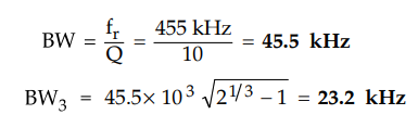
Determine the bandwidth of a 3 stage cascaded single tuned amplifier if the
resonant frequency is 455 kHz and the loaded Q of each stage is 10.
AU
: ECE : May-04
Ans.
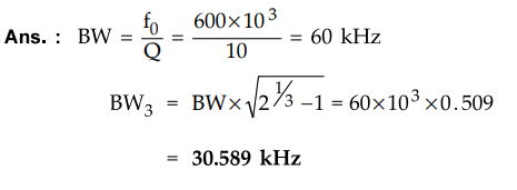
Q.39
If the resonant frequency and the effective loaded Q of a single tuned
amplifier are 600 kHz and 10 respectively, calculate the bandwidth of a 3 stage
cascaded synchronously tuned single tuned amplifier.
Ans.
Q.40
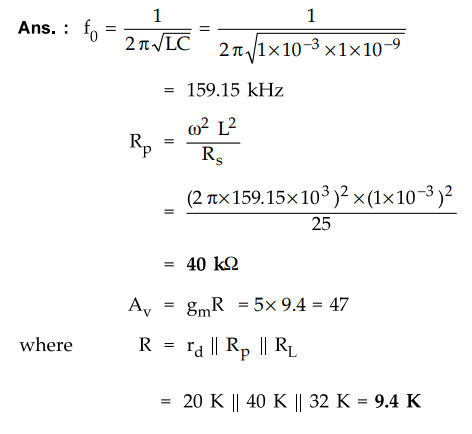
A single tuned amplifier using n channel JFET with gm = 5 mAJV and rd = 20 k
Ω,
has tank circuit with L = 1 mH, series resistance of the coil Rs = 25 Q and C =
1 nF. Calculate the voltage gain at resonance if = 32 k Ω.
AU
: ECE : May-05
Ans.
:
Q.41 What is the effect of Q on the resonance
circuit ?
AU
: ECE : Dec.-05, 07
Ans.
:
Increase in Q reduces bandwidth and increases selectivity of the resonance
circuit.
Q.42
Discuss briefly about neutralization in tuned amplifiers.
AU
: ECE : Dec.-05
Ans.
:
The effect of collector to base capacitance of the transistor is neutralized by
introducing a signal that cancels the signal coupled through collector base
capacitance. This process is called neutralization.
Q.43
Mention two applications of tuned amplifiers.
AU
: ECE : Dec.-07, 08, May-08
Ans.
:
The important applications of tuned amplifiers are as follows :
1.
Tuned amplifiers are used in radio receivers to amplify a particular band of
frequencies for which the radio receiver is tuned.
2.
Tuned class B and class C amplifiers are used as an output RF amplifiers in radio
transmitters to increase the output efficiency and to reduce the harmonics.
3.
Tuned amplifiers are used in active filters such as low pass, high pass and
band pass to allow amplification of signal only in the desired narrow band.
Q.44
What is the need for neutralization in tuned amplifiers ?
AU
: ECE : Dec.-08, 09, 10,15, May-13
Ans.
:
In tuned RF amplifiers, at high frequencies centered around a radio frequency
the inter junction capacitance between base and collector, Cbc of the
transistor becomes dominant, i.e. its reactance becomes low enough to be
considered. As reactance of Cbc at RF is low enough it provides the feedback
path from collector to base. If this feedback is positive, the circuit is
converted to an unstable one, generating its own oscillations and can stop
working as an amplifier. In order to prevent oscillations without reducing the
stage gain neutralization is used in tuned amplifiers.
Q.45
Draw the ideal response and actual response of tuned amplifiers. (Refer section
8.8.1)
AU
: ECE : May-09
Q.46
Define gain bandwidth product of a tuned amplifier.
Ans.
:
A gain bandwidth product of a tuned amplifier is defined as a product of 3 dB
bandwidth and the gain at response of the tuned amplifier.
Q.47
A tuned amplifier is designed to receive AM broadcast of speech signal at 650
kHz. What is needed Q for amplifier ?
Ans
.:
Given
: fc = 650 kHz
Assume
maximum modulating frequency
for
AM broadcast speech signal = 3 kHz.
Bandwidth
= 2 fm = 2 × 3 = 6 kHz.
We
have, Q = fr / BW = 650 kHz / 6 kHz = 108.33
Q.48
Draw the circuit for narrow band neutralization. (Refer Fig. 8.10.3)
Q.49
A tuned circuit has resonant frequency of 1600 kHz and bandwidth of 10 kHz.
What is the value of its Q-factor ?
Ans.
:
Given : fr =1600 kHz and BW = 10 kHz
Q
= fr / BW = 1600 / 10 = 160
Q.50
List the features of large signal amplifiers. (Refer section 8.13.1)
Q.51
Compare small signal and large signal amplifiers. (Refer section 8.13.4)
Q.52
State the position of Q point for class A, B and C amplifiers.
Ans.
: For class A : Q point is at the midpoint of the load
line.
For
class B : Q point is on the X-axis i.e. VCE axis.
For
class C : Q point is below the X-axis i.e. VCE
axis.
Q.53
Draw the nature of the output current flow for class A, B, C and AB amplifiers.
Ans.
:
Refer last row of the Table 8.15.1.
Q.54
List the various methods of improving CMRR.
AU
: Dec.-14, May-16
Ans.
:
1.
Using current source circuit insted of RE.
2.
Using current mirror circuit insted of RE.
3.
Using active load i.e. current source circuit as a load.
Q.55
Write down the need of cascading the amplifiers.
(Refer
section 8.1.1)
Q.56
CMRR of an amplifier is 100 dB, calculate common mode gain, if the differential
gain is 1000
AU
: Dec.-16
Ans.
:
CMRR = 100 dB, Ad = 1000
CMRR
in dB = 20 Log CMRR
i.e. CMRR = Antilog = l00 / 20 = 1 × 10⁵
CMRR
= Ad/Ac
Ac
= Ad / CMRR = 1000 / 1 × 10⁵
Q.57
Define conversion efficiency of power amplifier.
AU
: Dec.-16
Ans.
:
The ratio of a.c. power output to d.c. power input to a power amplifier is
called its conversion efficiency,
%
conversion efficiency = Pac / PDC × 100
Q.58
Differentiate between power transistor and signal transistor.
Ans.
: Difference between power transistor and small signal transistor
•
Power transistors are capable of carrying higher currents than small signal
transistors.
•
Power transistors come in metal packages, usually have bigger body, body itself
is a heat sink. Small signal transistors come in plastic/metal packages.
•
Power transistor has a vertical structure and small signal transistor has
horizontal structure.
•
In power transistor quasi saturation region is present which is absent in the
small signal transistor.
•
In power transistor there is an inclusion of drift layer which is not there in
the small signal transistor.
•
Usually a "small signal" transistor is expected to operate in
"small signal mode" which is a signal level "sufficiently
small" to be mostly linear. Power transistors are not necessarily operated
in this small signal mode.
Q.59
Define differential mode signals of a differential amplifier.
Ans.
:
The difference between the two input signals applied to two differential input
terminals of a differential amplifier is called differential mode signal of a
differential amplifier.
Electron Devices and Circuits: Unit IV: Multistage and Differential Amplifiers : Tag: : Multistage and Differential Amplifiers | Electron Devices and Circuits - Two Marks Questions with Answers
Related Topics
Related Subjects

Electron Devices and Circuits
EC3301 3rd Semester EEE Dept | 2021 Regulation | 3rd Semester EEE Dept 2021 Regulation