Linear Integrated Circuits: Unit II: Characteristics of Op-amp
Two Marks Questions with Answers
Characteristics of Op-amp | Linear Integrated Circuits
Linear Integrated Circuits : Unit II: Characteristics of Op-amp : Two Marks Questions with Answers
Two Marks Questions with Answers
Q.
1 One op-amp has CMRR of 100 dB and other has CMRR of 40 dB. Which you will
prefer and why?
Ans.
: The
dB value of the CMRR is 20 Log (CMRR). More the value of CMRR, better is the
performance of the differential amplifier as it greatly rejects the unwanted
common mode signals and produce the output almost proportional to the
difference voltage at its input terminals. Thus the differential amplifier with
higher CMRR is always preferred so that having CMRR 100 dB is preferred over
the other having CMRR of 40 dB.
Q.
2 What is an operational amplifier ?
Ans.
: The
operational amplifier is basically an excellent high gain differential
amplifier. It amplifies the difference between its two inputs. Due to its use
in performing mathematical operations it has been given a name operational
amplifier.
Q.
3 Draw the op-amp symbol and state its important terminals.
Ans.
:
For the op-amp symbol, refer the Fig. 2.2.1. The important terminals are,
1.
Positive supply 2. Negative supply 3. Output 4. Inverting input 5. Noninverting
input.
Q.
4 State the various blocks of IC op-amp.
Ans.
:
1. Internal stage 2. Intermediate stage
3.
Level shifting stage 4. Output stage.
Q.
5 Which circuits are commonly used for the various stages of an 1C op-amp ?
Ans.
:
1.
Internal stage : Dual input balanced output differential
amplifier.
2.
Intermediate stage : Multistage amplifiers without coupling
capacitors and single ended
3.
Level shifting stage : Various transistor circuits to
reduce the d.c. output level.
4.
Output stage: Push-pull complementary symmetry
amplifier in Class AB operation.
Q.
6 List the requirements of the internal stage of IC op-amp.
Ans.
:
1. High voltage gain 2. High input impedance 3. Two input terminals
4.
Small offset voltages 5. Small offset currents 6. High CMRR.
Q.
7 Why level shifting is required in op-amp ?
Ans.
:
As coupling capacitors are not used in the intermediate stage of the op-amp,
the d.c. biasing voltage level propagates through the chain of the amplifiers.
Finally it appears as a significant d.c. component present at the output along
with the desired a.c. output. Such a d.c. level distorts the output and limits
the maximum output voltage swing. Hence it is necessary to reduce this d.c.
level before the output stage for which level shifting circuit is used.
Q.8
List the requirements of the output stage of IC op-amp.
Ans.
:
1. High output voltage swing 2. High output current swing 3. Low output
impedance 4. Low quiescent power dissipation 5. Various
protection circuits.
Q.9
List the important characteristics of ideal op-amp.
Ans.
:
1. Infinite voltage gain 2. Infinite input impedance 3. Zero output impedance
4.
Infinite bandwidth 5. Infinite CMRR 6. Infinite slew rate 7. Zero PSRR
Q.10
Draw the equivalent circuit of practical op-amp.
Ans. :

Q.
11 What is input offset voltage ?
Ans.
:
When both the input terminals of the op-amp are grounded, ideally the output
should be zero. But practically op-amp produces the small output voltage. To
nullify this voltage, some voltage is required to be applied to either of the
two input terminals in the particular direction. This voltage is called input
offset voltage.
How
much voltage, to which input and with what polarity is specified by the
manufacturer in the data sheet of the op-amp.
Q.12
What is input bias current and input offset current ?
Ans.
:
The base currents of the transistors used in the input stage of the
differential amplifier are practically finite and the two currents differ in
magnitude as perfect matched transistors are not possible in practice. These
currents are responsible for the input bias current and input offset current of
op-amp.
The
input bias current is the average of the two base currents Ib,and Ib2 while the
input offset current is the difference between the two base currents Ib,^d Ib2.
Q.13
What is output offset voltage ? Which parameters are responsible to produce it
?
Ans.
:
The output voltage present when both the input terminals of the op-amp are
grounded is called output offset voltage. The input offset voltage, input bias
current and input offset current are responsible to produce output offset
voltage.
Q.
14 What is thermal drift ?
Ans.
:
The dependence of the op-amp parameters on the temperature is indicated by a
factor called temperature drift. The change in the op-amp parameter
corresponding to the change in the temperature is defined as the thermal drift
of that parameter. Thus Δ Vios / ΔT is called input offset voltage
temperature drift.
Q.
15 What is PSRR ? What should be its ideal value ?
Ans.
:
PSRR is power supply rejection ratio. It is defined as the change in the input
offset voltage due to the change in one of the two supply voltages when other
voltage is maintained constant Its ideal value should be zero.
Q.
16 What is slew rate ? State slew rate equation.
Ans.
:
The maximum rate of change of output voltage with respect to time is called
slew rate of the op-amp.

The
slew rate equation is, S = 2π fVm V / sec
Q.17
Draw the typical frequency response of the op-amp.
Ans. : Refer the Fig. 2.15.2 of the section 2.15. The students may draw it without semilogpaper only indicating the nature of the two plots.

Q.18
Compare the ideal and practical op-amp characteristics.
Ans.
:

Q.19
What is frequency response of the op-amp ?
Ans.
:
The plot showing the variations in magnitude and phase angle of the gain of
op-amp due to the changes in the input frequency is called the frequency
response of the op-amp.
Q.20
What is frequency compensation ?
Ans.
:
The method of modifying loop gain frequency response of the op-amp so that it
behaves like single break frequency response which provides sufficient positive
phase margin is called frequency compensation technique.
Q.21
List the methods used to provide the external frequency compensation.
Ans.
:
The methods used to provide the external frequency compensation are,
1.
Dominant pole compensation
2.
Pole-Zero compensation
3.
Feed-Forward compensation.
Q.
22 Define unity gain bandwidth of an Op-amp. What is its value for IC741 ?
Ans.
:
At a certain frequency, the open loop gain reduces to 0 dB. This indicates that
20 log | AOL(f) | is 0 dB i.e. | AOL(f) | = 1. Such a
frequency at which magnitude of the open loop gain is unity is called gain
cross-over frequency or Unity Gain Bandwidth (UGB). It is also called closed
loop bandwidth. For IC 741, UGB is about 1 MHz.
Q.23
Find the maximum frequency for an op-amp with sine wave output voltage of 10 V
peak and slew rate is 2 V/µs.
Ans
: 
Q.24
In what way 741S is better than 741 ? Dec.-03
Ans.
S
stands for slew rate. Thus 7418 has higher slew rate than 741.
Q.25
Draw a circuit using operational amplifier to convert square wave to triangular
wave.
Dec.-04
Ans. : This circuit is integrator circuit. Refer section for the circuit of an integrator.
Q.26
What is a practical op-amp? Draw the equivalent circuit. (Refer section 2.11)
Q.27
Define slew rate and CMRR. (Refer sections 2.13.2 and 2.4.3)
Q.28
Draw the circuit diagram of differentiator using op-amp. (Refer section 2.30)
Q.29
The two input bias currents of an operational amplifier are 22 μA and 26 μА.
What is the value of input offset current? Input bias current ? May-07
Ans.
:

Q.30
Why operational amplifier open loop configurations are not used in linear
applications ? May-07
Ans.
: Op-amp has a saturable property in open loop mode. Its output
saturates at Vsat which is 0.9 times its supply voltages. Its open
loop gain is very very high, of the order of 2 × 10⁵. Hence for very
small range of input, of the order of few µV the output varies linearily with
the input. This range is not sufficient for the practice linear applications.
Hence the open loop op-amp is not used in the linear applications.
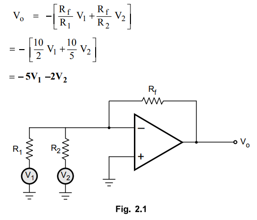
Q.31
Find Vo for the circuit shown Rf = 10 kΩ, R1 =
2 kΩ, R2 = 5kΩ.
Ans.
:
This is inverting summing amplifier with the output expression as
Q. 32 Define slew rate. What is its significance ?
(Refer
section 2.13.2)
Q.
33 What is the need for compensating network in op-amps ?
Ans.
:
Due to slight mismatch in the first stage of op-amp, there exists input offset
voltage and input bias current. Both are responsible to produce output offset
voltage. This voltage must be ideally zero. For making this voltage as small as
possible, the compensating network is necessary in op-amps.
Q.
34 An op-amp data sheet gives 15 V power bandwidth of 25 kHz. What is the slew
rate ?
Ans.
:

Q.
35 Discuss the cause of output offset voltage in op-amp.
Ans.
:
The output offset voltage (Voos) is the difference between d.c.
voltage present at the output terminals when both the input terminals are
grounded. The two main causes for output offset voltage in op-amp are,
1.
Input offset voltage (Vios) 2. Input bias current (Ib)
The
output voltage caused by input offset voltage can be either positive or
negative with respect to ground. Similarly, the output voltage caused by input
bias current can be either positive or negative with respect to ground. If
these voltages are of the same polarity then the output offset voltage is
large.
The
output offset voltage due to these two parameters are given by,
Voos
= (l + Rf / R1) Vios + Ib Rf
where
Rf is feedback resistance and Rx resistance in series with the
source.
To
make this Voos as small as possible, compensating network is used in
the op-amps.
Q.36
Draw the circuit diagram of an op-amp integrator. Mention its applications.
(Refer
section 2.29)
Q.
37 Compare ideal and practical characteristics of an op-amp.
(Refer
section 2.19)
Dec.-08
Q.
38 Design an amplifier with a gain of -10 and input resistance of 10 kΩ.
Ans.
:
The gain is -10 hence it is inverting amplifier and its input resistance is R1
= 10 kΩ.
Gain
= Rf / R1
-
10 = - Rf / 10
Rf
= 100 kΩ
The
designed circuit is shown in the Fig. 2.2.

Q.39
Give the ideal characteristics of op-amp and give its equivalent circuit.
(Refer
sections 2.10 and 2.11)
Q.40 Draw the circuit diagram of an integrator and give its output equation.
Ans.
:
Refer Fig. 2.29.1 of the section 2.29. The output equation of an integrator is,
Q.41
What are the different kinds of packages of 1C 741 ?
Ans.
:
The three packages in which IC741 op-amp is available are,
1.
Metal can package (TO)
2.
Dual in line package (DIP) 3. Flat package.
Q.
42 Mention two linear and two non-linear applications performed by an
operational amplifier.
Ans.
:
The linear applications are inverting amplifier, non-inverting amplifier,
voltage follower, integrator, differentiator, instrumentation amplifier etc.
The
non-linear applications are comparator, Schmitt trigger, zero crossing
detector, log amplifier, precision rectifier etc.
Q.
43 State the two realistic simplifying assumptions used for the op-amp.
Ans.
:
The two realistic simplifying assumptions used for the op-amp are,
1.
The input current of the op-amp is always zero.
2.
Concept of virtual ground which says that the two input terminals of the op-amp
are always at the same potential. Thus if one is grounded then other can be
assumed to be at ground potential, which is called virtual ground.
Q.44
Draw the circuit diagram of inverting amplifier and state gain. expression for
its gain
Ans. : Refer section 2.21. Gain = - Rf / R1 .
Q.
45 Draw the circuit diagram of
non-inverting amplifier and state expression for its gain.
Ans.
: Refer section 2.22. Gain = 1 + (Rf
/ R1 )
Q.46 When inverting amplifier is called phase
inverter ?
Ans.
: When the gain of the inverting
amplifier is unity and it is used to
change the phase of the input to produce the output then it is called phase
inverter.
Q.47
What is sign changer or inverter ?
Ans.
:
If in the inverting amplifier if Rf is made equal to R|then gain of the
amplifier becomes -1. Thus the circuit changes the sign of the input i.e. phase
of the input without changing its magnitude at its output. This circuit is
called sign changer or phase inverter.
Q.48
How an op-amp can be used as a voltage follower ?
(Refer
section 2.24)
Q.49
State the advantages of voltage follower.
Ans.
:
1)
Very large input resistance, of the order of MQ.
2)
Low output impedance, almost zero. Hence it can be used to connect high
impedance source to a low impedance load, as a buffer.
3)
It has large bandwidth.
4)
The output follows the input exactly without a phase shift.
Q.
50 Draw the circuit diagram of inverting summer.
(Refer
Fig. 2.27.1 of section 2.27.1)
Q.51
Draw the circuit diagram of non-inverting summer.
(Refer
Fig. 2.27.2 of section 2.27.2)
Q.52
How to obtain the average circuit from the inverting summer ?
Ans.
:
In an inverting summer if the values of resistances are selected such that R1
= R2 = R and Rf = R/2 then the output is the average of
the two inputs applied to the circuit.
Q.53
Draw the circuit diagram of subtractor.
(Refer
Fig. 2.28.1 of the section 2.28)
Q.
54 Draw the input and output waveforms for an integrator for step and
sinusoidal type of inputs.
(Refer
section 2.29.2)
Q.
55 State the errors in an ideal integrator.
Ans.
:
1.
The output is likely to saturate in absence of input.
2.
The output may be distorted due to the error voltage.
3.
The bandwidth is very small.
4.
It can be used only for small range of frequencies.
Q.
56 Draw the circuit diagram of practical integrator circuit.
(Refer
Fig. 2.29.8 of the section 2.29.4)
Q.
57 List the applications of integrator circuit.
Ans.
:
i) In the analog computers, ii) In solving differential equations, iii) In
analog to digital converters, iv) Various signal wave shaping circuits, v) In
ramp and triangular waveform generators.
Q.
58 Draw the circuit diagram of an ideal differentiator. Write expression for
its output.
Ans . :
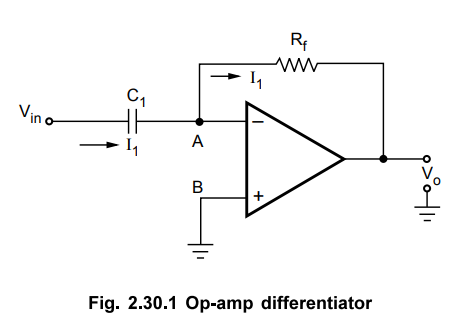
Its output expression is ,
Vo
= - C1 Rf (dVin
/ dt)
Q.
59 Draw the input and output waveforms for differentiator for step and square
type of inputs.
(Refer section 2.30.2)
Q.
60 State the errors in an ideal differentiator.
Ans.
:
1.
The gain increases as the frequency increases hence the circuit becomes
unstable at high frequency.
2.
The input impedance decreases as the frequency increases hence circuit becomes
sensitive to the noise which can completely override the differential output.
Q.
61 Draw the circuit diagram of the practical differentiator circuit.
(Refer
Fig. 2.30.6 of the section 2.30.4)
Q.
62 List the applications of differentiator circuit.
Ans.
:
i) In the wave shaping circuits, ii) To detect high frequency components in the
input, iii) As a rate of change detector in the FM demodulators.
Q.
63 In an inverting amplifier the values of Rf and R1 are 100 kΩ and 10 kΩ
respectively. What is the gain of the amplifier?
Ans
:
Gain of the inverting amplifier is given by – Rf / R1 = -
100 / 10 = -10.
Q.
64 How will you increase the output of a general purpose op-amp ?
Ans.
:
A simple method of increasing the output current of a general purpose op-amp is
to connect a power booster circuit in series with the op-amp. This is shown in
the Fig. 2.3

Q
65 List any four non ideal dc characteristics of op-amp.
May-12
i)
Input bias current iii) Input offset
current
iii)
Input offset voltage iv) Output offset
voltage.
Q.
66 Calculate the value of the current I flowing through resistance R in the
operational amplifier circuit shown in Fig. 2.4.

Ans.
:
Due to the concept of virtual ground, the non-inverting terminal voltage must
be same as inverting terminal.
VB
= VA = 5 V.. Virtual ground
As
no current can flow into the op-amp, current through 1 kΩ is I only.

Q.
67 Define CMRR.
Ans.
:
The ratio of the differential voltage gain Ad to the common mode voltage gain Ac
is called CMRR of an op-amp.
Q.
68 What is V to I converter ?
Ans.
:
The circuit in which the output load current is proportional to the input
voltage is called V to I converter. Mathematically it is given by IL
∝ Vin
Q.
69 What is I to V converter ?
Ans.
:
The circuit in which the output voltage is proportional to the input current is
called I to V converter. Mathematically it is given by Vo oc Iin.
Q.
70 Draw the circuit of current to voltage converter using op-amp and bring out
the relation. State one application.
(Refer
section 2.26)
Q.
71 State the applications of voltage to current converter.
Ans.
:
1.
Low voltage d.c. voltmeter 2. Low voltage a.c. voltmeter
3.
Diode tester and match finder 4. Zener diode tester.
Q.
72 State the applications of current to voltage converter.
Ans.
:
1. Photodiode detector 2. PhotoFET detector.
Q.
73 Draw the frequency response characteristic of an A.C. integrator and
indicate the part where it behaves as a true integrator.
Ans. : The frequency response of the practical integrator is shown in the Fig. 2.5.

Q.
74 State the causes for slew rarte in an operational amplifier ? How it is indicated?
Ans.
:
The causes of slew rate are,
1.
Limited charging rate of the compensating capacitor.
2.
Current limiting of the internal stages of an op-amp.
3.
Saturation of the internal stages of an op-amp.
The
slew rate is indicated as, S = dVo / dt | maximum
Q 76 A
100 pF capacitor has a maximum charging current of 100 microamps. What is the
slew rate ?
Ans : S = Imax / C = 100 × 10-6 / 100 × 10-12 = 1 × 10⁶ V/sec = 1 V/µ sec
Q.77
Explain how the average circuit can be derived from the summer.
(Refer
section 2.27)
Q. 78 Why IC 741 is not used for high frequency applications ?
Ans.
:
Due to predominant capacitance effect, the slew rate of IC 741 is very small.
At high frequencies, the output gets distorted due to small slew rate. Hence IC
741 is not used for high frequency applications.
Q.79
What is integrator ?
Ans.
:
An integrator is a circuit which produces output which is integration of the
input applied to it. Then refer Q.40.
Q.80
Draw the circuit diagram of a symmetrical emitter coupled differential
amplifier.
(Refer Fig. 2.5.2 of section 2.5)
Q.
81 For the circuit diagram shown below determine the output voltage V0.
Ans.
:
It is a subtractor with

Q.
82 What is the drawback of IC 741?
Dec-17
Ans.
:
The main drawback of IC 741 is that its slew rate is small hence it cannot be
used for high frequency applications. Compared to modem op-amp ICs, 741 has low
input impedance, high offset voltage and current and minimum power supply
required is ± 10 V. The drift in parameters with respect to temperature is
high.
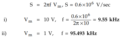
Q.
83 The slew rate of an op-amp is 0.6 V/micro sec. What is the maximum
undistorted sine-wave that can be obtained for a 10 V peak and 1 V peak ?
May-18
Ans.
:
From slew rate equation,
Linear Integrated Circuits: Unit II: Characteristics of Op-amp : Tag: : Characteristics of Op-amp | Linear Integrated Circuits - Two Marks Questions with Answers
Related Topics
Related Subjects

Linear Integrated Circuits
EE3402 Lic Operational Amplifiers 4th Semester EEE Dept | 2021 Regulation | 4th Semester EEE Dept 2021 Regulation