Linear Integrated Circuits: Unit III: Applications of Op-amp
Two Marks Questions with Answers
Applications of Op-amp | Linear Integrated Circuits
Linear Integrated Circuits : Unit III: Applications of Op-amp : Two Marks Questions with Answers
Two Marks Questions with Answers
Q.1
What is the disadvantage of dual slope ADC ?
Ans.
:
The only disadvantage of dual slope ADC is its speed which is low.
Q.2
An A/D converter has a conversion time of 1 microseconds. Calculate the maximum
frequency at which it can be used.
Ans.
:
According to Nyquist criteria sampling rate should be atleast two-in-one clock
cycle. To complete conversion of two samples we require 2µs. Therefore, the
maximum frequency at which we can use A/D converter is 1 / 2µs = 500kHz.
Q.3
An 8 bit D/A converter has output voltage range of 0-5 volt. Calculate the
change in its output voltage when the least significant bit of the input
changes.
Ans
:
Change in output voltage = 5 / 28 – 1 = 19.6 mV
Q.4 Compare the methods of conversion of digital to analog signal and explain the characteristics of DAC IC.
(Refer section 3.25)
Q.5
What is the difference between a sawtooth wave and a triangular wave ?
May-06
Ans.
:
The triangular wave consists of two straight lines having opposite slopes as
shown in the Fig. 3.1 (a). In sawtooth there is one straight line of positive
slope and other vertical line as shown in the Fig. 3.1 (b).
Q.6
What is a sample and hold circuit ? Why it is needed ?
(Refer
section 3.24)
Q.7
What are the advantages of active filters ?
OR
Why
active filters are preferred.
(Refer
section 3.4.1)
Q.8
Which type of A/D converter is used in digital multivibrator ? Why ?
Ans
:
Dual slope A/D converter is used in digital multivibrator.
Q.9
Compare the conversion times for tracking and successive approximation A-D
converters.
Ans.
:
The tracking ADC requires a DAC an up/down counter, with the comparator which
controls the direction of count. Counting will be up or down depending on
whether the DAC output is below or above Vi Whenever the DAC output
crosses y, the comparator changes state, and this can be taken as the EOC
command. Clearly, the conversion times will be relatively short only if Vi
doesn't change too radically between consecutive conversions. In the worst-case
situation of a full-scale input change, the conversion will take (2n
-1) clock periods.
Q.10 Sketch the circuit of an op-amp employed as, a non-inverting zero crossing detector, along with input and output waveforms.
(Refer
section 3.12.4.1)
Q.11
List any four important applications of a comparator.
Ans.
:
1.
Zero crossing detector
2.
Level detector
3.
Window detector
4.
Duty cycle controller
5.
Pulse generator
6.
Time marker generator.
Q.12
What is the advantage of active op-amp based clipper over passive clipper ?
May-08
Ans.
:
In passive clipper, the diode cannot work as an ideal diode due to voltage drop
across it. But in active clipper, the drop across diode gets divided by the
open loop gain of the op-amp which is very high. Hence diode becomes ON
instantly and behaves as an ideal diode. This causes a precise clipping action.
Q.13
How many resistors are required in a 10-bit weighted resistor D/A converter ?
Ans.
: 10
resistors are required in a 10-bit weighted resistor D/A converter.
Q.14
List the important specifications of A/D and D/A converters.
(Refer
sections 3.25.1 and 3.26.1)
May-08
Q.15
An eight bit DAC produces an 'output' voltage of 0 V corresponds to an input
bit sequence '00000000'. If the DAC is connected for a basic step increment of
10 mV, what would be the output voltage for the input sequence, '11111111' ?
May-08
Ans.
: 10mV
× 225 = 2550 mV = 2.55V
Q.16
What is a zero crossing detector ?
Ans
:
A circuit which detects the crossing of zero level by the input signal is
called a crossing detector. An op-amp comparator is used as a zero crossing
detector.
Q.
17 Which is the fastest ADC ? Give reason.
(Refer
section 3.26.2)
Q.18
What are the basic requirements of a good instrumentation amplifier ?
(Refer
section 3.1.1)
Q.19
Find the resolution of a 8 bit D/A converter.
Ans
: For
8 bit DAC, n = 8
Resolution
= 2n = 256
Q.20
An 8 bit DAC has a resolution of 20 mV/bit. What is the analog output voltage for
the digital input code 00010110 (the MSB is the left most bit) ?
Ans
:
(10110)2 = (22)10
Vo
= 20 mV × 22 = 440 mV
Q.21
Draw the circuit diagram of op-amp based positive clipper.
(Refer
section 3.21.1)
Q.22
What is the need for an instrumentation amplilfier ?
Ans.
:
The output level of most of the transducers is very low. In practical systems
it is necessary to amplify the level of such signals rejecting the noise and
the interference. Hence the amplifiers with high CMRR, high input impedance for
avoiding loading and low power consumption are necessary. These amplifiers are
nothing but instrumentation amplifiers.
Q.23
Define conversion time of ADC.
Ans.
:
It is the total time required to convert an anlog signal into its digital
output.
Q.24
What is instrumentation amplifier ?
Ans.
:
In many practical circuits it is necessary to amplify low level signals
obtained from devices like transducer. The special amplifiers which are
basically difference amplifiers are used for low level signal amplification,
having high CMRR, high input impedance and low power consumption are called
instrumentation amplifiers.
Q.25
State the important features of an instrumentation amplifier.
Ans
:
The important features of an instrumentation amplifier are,
1.
It is finite, accurate and stable.
2.
Easy gain adjustment
3.
High input impedance
4.
Low output impedance
5.
High CMRR.
6.
Low power consumption
7.
Low thermal drift
8.
High slew rate.
Q.26
Draw the circuit diagram of three op-amp instrumentation amplifier.
(Refer
section 3.1.2)
Q.27
Why active guard drive is necessary for an instrumentation amplifier ?
Ans.
:
Practically the common ground bus is shared by variety of circuits. Due to
ground loop interference additional voltage drop gets inserted which may cause
error in low level measurements. Due to distributed cable capacitances there is
degradation of CMRR. The active guard drive eliminates all these problems and
hence necessary for an instrumentation amplifier.
Q.28
State any four applications of an instrumentation amplifier.
Ans.
:
1. Temperature controller 2. Data acquisition systems
3.
Temperature indicator 4. Light intensity meter 5. Analog weight scale
Q.29
What is comparator ?
Ans.
:
The open loop op-amp can be used as a comparator. The comparator is a circuit
which compares a signal voltage applied at one of the input terminals of the
op-amp with a known reference voltage applied at the other input terminal and
produces the saturation voltage either high or low, depending on which input is
higher.
Q.30
Draw the input and output waveforms of a non-inverting comparator if input is
purely sinusoidal.
(Refer
section 3.12.1)
Q.31
Draw the input and output waveforms of inverting comparator if input is purely
sinusoidal.
(Refer
section 3.12.2)
Q.32
List any five characteristics of comparator.
Ans.
:
While using op-amp as a comparator along with the op-amp parameters following
characteristics of a comparator must be considered.
1.
Accuracy 2. Logic threshold 3. Response time 4. Positive and negative
output level 5. Strobe current 6. Strobe
release time.
Q.33
What is logic threshold voltage level ?
Ans.
:
It is the voltage level at the output of a comparator at which the connected
digital device changes its state. For TTL it is approximately 1.2 V while for
CMOS it is 2.5 V.
Q.34
Enlist the applications of comparators.
Ans.
:
1. Zero crossing detector 2. Level detector 3. Window detector 4. Duty cycle
controller 5. Pulse generator 6. Time marker generator .
Q.35
What is Schmitt trigger ?
Ans.
:
The comparator circuit used to avoid unwanted triggering using a positive
feedback is called a regenerative comparator or Schmitt trigger.
Q.36
What is a precision rectifier ? How it differs from conventional rectifier ?
Ans.
:
In conventional rectifier, as long as input does not exceed the cut-in voltage
of the diode, it does not conduct. Due to this the output is distorted
producing crossover distortion. For the input between ± 0.7 V, the output
remains zero which is main limitation of the conventional rectifier. Hence the
voltages below 0.7 V can not be rectified. In precision rectifier the op-amp is
used. The open loop gain of the op-amp is very large. Hence for very small
amount of the input of the order of few mV, it produces the large output which
can easily make the diode conduct. Thus the diode conducts for very small input
voltages of the order of millivolts. Hence the precision rectifiers are very
precise.
Q.37
Draw the circuit diagram of half wave precision rectifier.
Dec.-09
(Refer
section 3.27.1)
Q.38
Draw the circuit diagram of full wave precision rectifier.
(Refer
section 3.27.2)
Q.39
Draw the circuit diagram of log amplifier using transistor and write its output
expression.
Ans
:
Refer section 3.2.1. Its output expression is Vo = - VT
ln[ Vin / Vref]
Q.40
What is an antilog amplifier? Write its output expression.
Ans.
:
The circuit which produces the output which is proportional to the antilog of
the input is called antilog amplifier. Such op-amp antilog amplifier produces
the output proportional to the exponential of the input which is nothing but
its antilog. Its output expression is, Vo = Vref e Vin/
η
VT
Q.41
Why temperature compensation is required for the log amplifiers ?
Ans.
:
The reverse saturation current Io for the diode changes with temperature. In
fact it doubles for every ten degree celcius rise in the temperature. Similarly
the emitter saturation current varies significantly from one transistor to
other and also with the temperature. Hence it is very difficult to set the term
\ef for the circuit. The term VT which is kT also changes with temperature,
which appears in the final equations. Thus temperature affects the performance
and accuracy of the basic logarithmic amplifier circuit. Hence it is must to
provide some sort of temperature compensation to reduce the errors.
Q.42
An a.c. signal has got a magnitude of 0.1 volt peak to peak. Suggest a suitable
half wave rectifier for this signal.
Ans.
:
0.1 V peak to peak is less than 0.7 V which is cut-in voltage of diode hence
conventional rectifier is not suitable. For such a case precision rectifier
using op-amp and diode is suitable.
Q.43
What is filter?
Ans.
:
A filter is a circuit that is designed to pass a specified band of frequencies
while attenuating all the signals outside that band. The filter circuit using
the active elements such as op-amp and transistors along with the passive elements
like R, L and C are called active filters.
Q.44
Sketch the frequency responses of low pass, high pass, band pass and band
elimination filters.
(Refer
section 3.4.2)
Q.45
Draw the circuit diagram of first order low pass Butterworth filter.
(Refer
section 3.6)
Q.46
What is a rate of decrease in gain for first order and second order low pass
Butterworth filters?
Ans.
:
The rate of decrease in gain for first order Butterworth filter is - 20
dB/decade while for second order low pass Butterworth filter it is - 40
dB/decade.
Q.47
What is frequency scaling?
Ans.
:
Many times when the filter is designed, practically it is necessary to change
its cut-off frequency. The method used to change the cut-off frequency of the
filter is called frequency scaling.
Q.48
Draw the circuit diagram of second order low pass Butterworth filter.
(Refer
section 3.7)
Q.49
Draw the circuit diagram of wide band pass filter.
(Refer
section 3.10.1)
Q.50
State the expression for the overall gain of wide band pass filter.
Ans
:
The expression for the overall gain of wide band pas filter is,

where
AFT = Total pass band gain, f
= Input frequency in Hz
fL
= Lower cut off frequency in Hz fH = Higher cut off frequency in Hz
and
AFT = A1A2
where
A1 = Gain of high pass
section and A2 = Gain of low pass section
Q.51
Draw the circuit diagram of narrow band pass filter.
(Refer
section 3.10.2)
Q.52
State the disadvantages of passive filters.
Ans.
:
The disadvantages of passive filters are,
i)
Number of elements required are more,
ii)
The filter gain and frequency adjustments can not be easily obtained,
iii)
Cause loading effect,
iv)
Without inductors high value of Q can not be achieved,
v)
At low frequencies the necessarily high values of L and C can result in an
inconveniently large size and weight which makes them bulky,
vi
) The design procedures are complex,
vii)
Often exhibits a significant loss.
Q.53
What is the roll off rate for a third order low pass filter.
Ans.
:
The roll off rate of first order filter is - 20 dB/decade hence the roll off
rate of third order filter is - 20 × 3 = - 60 dB/decade.
Q.54
Draw the neat circuit diagram of R-C phase shift oscillator using Op-amp.
(Refer
section 3.17)
Q.55
State the advantages and disadvantages of RC phase shift oscillator.
(Refer
sections 3.17.4 and 3.17.5)
Q.56
Draw the neat circuit diagram of Wien bridge oscillator using Op-amp.
(Refer
section 3.18)
Q.57
State the advantages of Wien bridge oscillator.
(Refer
section 3.18.2)
Q.58
Compare R-C phase shift oscillator and Wien bridge oscillator circuits.
(Refer
section 3.19)
Q.59
What is monostable multivibrator circuit ?
Ans.
:
The circuit which produces a single pulse of specified duration in response to
each external trigger signal is called monostable multivibrator circuit. It has
only one stable state and it is also called one shot multivibrator.
Q.60
What is astable multivibrator circuit ?
Ans.
:
The circuit which has two quasi-stable states and which oscillates between
these two states without application of the trigger signal is called astable
multivibrator circuit. It is also called free running multivibrator.
Q.61
Draw the circuit diagram of monostable multivibrator circuit and state the
expression for its pulse width.
Refer
section 3.14. Its pulse width is given by,

Q.62
Draw the circuit diagram of astable multivibrator circuit and state the
expression for its frequency of oscillations.
Refer
section 3.15. Its frequency is given by,

Q.63
State the applications of monostable multivibrator.
Ans.
:
1. Frequency divider 2. Missing pulse
detector 3. Pulse width modulation 4.
Pulse position modulation 5. Linear ramp generator
Q.64
State the applications of astable multivibrator.
Ans.
:
1. Square wave generator 2. FSK
generator 3. Voltage controlled
oscillator
Q.65
State the Barkhausen conditions required for the oscillations.
Ans.
:
The conditions required for producing the oscillations are given by the
Barkhausen Criterion which states that :
1.
The total phase shift around a loop, as the signal proceeds from input through
amplifier, feedback network back to input again, completing a loop, is
precisely 0° or 360o, or of course an integral multiple of 2π
radians.
2.
The magnitude of the product of the open loop gain of the amplifier (A) and the
feedback factor β is unity i.e. | A β | =1.
Q.66
Draw the circuit of negative clipper circuit.
(Refer
section 3.21.2)
Q.67
What is clipper circuit ?
Ans.
:
The circuit which is used to clip off the unwanted portion of the input signal
above or below certain level, so as to produce the limited required output is
called a limiter circuit or clipper circuit.
Q.68
What is clamper circuit ?
Ans.
:
The circuit which is used to add a d.c. level as per the requirements, to the
a.c. output is called clamper circuit or d.c. restorer circuit.
Q.69
What is peak detector ?
Ans.
:
A peak detector circuit is one which notes and remebers the peak positive or
negative value of an input signal for an infinite period of time until it is
reset.
Q.70
Draw the peak detector circuit using an integrator.
(Refer
section 3.23)
Q.71
What is a sample and hold circuit ?
Ans.
:
The sample and hold (S/H) circuit that samples the value of the input signal in
response to a sampling command and hold it at the output until arrival of the
next command is called sample and hold (S/H) circuit. It samples an analog
input voltage in a very short period, generally in the range of 1 to 10 ps, and
holds the sampled voltage level for an extended period, which can range from a
few millisecond to several seconds.
Q.72
What is the need of sample and hold circuit ?
Ans.
:
For accurate analog to digital conversion the analog input voltage should be
held constant during the conversion cycle. The input voltage is kept constant
during conversion time using sample and hold circuit.
Q.73
Draw a sample and hold circuit.
(Refer
section 3.24)
Q.74
What is an analog switch ?
Ans.
:
The switch that connects or disconnects the analog input signal to the output
is called analog switch. JFET can be used as an analog switch.
Q.75
What is the acquisition time of a S/H circuit ?
Ans.
:
The acquisition time of a S/H circuit is the time required for the holding
capacitor CH to charge up to a level close to the input voltage during
sampling. The acquisition time for S/H circuit should be as low as possible.
Q.76
Which factors control the acquisition time of a S/H circuit 7
Ans.
:
The acquisition time of a S/H circuit depends on three factors :
•
RC time constant
•
Maximum output current of op-amp
•
Slew rate of op-amp
Q.77
Define aperture time.
Ans.
:
Because of propagation delays through the driver and switch, Vo will keep
tracking V some time after the inception of the hold command. This is the
aperture time.
Q.78
Define aperture uncertainty.
Ans.
:
Aperture uncertainty is the variation in aperture time from sample to sample.
Due to aperture uncertainty it is difficult to compensate aperture time by
advancing hold command.
Q.79
Define hold mode settling time.
Ans.
:
After the application of hold command, it takes a certain amount of time for Vo
to settle within a specified error band, such as 1 %, 0.1 % or 0.01 %. This is
the hold mode settling time.
Q.80
Define voltage droop.
Ans.
:
The leakage current causes voltage of the capacitor to drop down. This is
referred to as droop.
Q.81
What is feedthrough ?
Ans.
:
In the hold mode, because of stray capacitance across the switch, there is a
small amount of ac coupling between Vo and Vi This ac
coupling causes output voltage to vary with variation in the input voltage.
This is referred to as feedthrough.
Q.82
What are advantages of S/H circuits ?
(Refer
section 3.24.1)
Q.83
State the application of S/H circuits.
(Refer
section 3.24.2)
Q.84
What is A/D and D/A converter 7
Ans.
:
The circuit that performs conversion of analog signal into digital signal is
called analog to digital (A/D) converter. On the other hand, the circuit that
performs conversion of digital signal into analog signal is called digital to
analog (D/A) converter.
Q.85
Define : Resolution of a D/A converter.
Ans.
:
• Resolution is the number of different analog output values that can be
provided by a DAC. For an n-bit DAC
Resolution
= 2n ... (1)
•
Resolution is also defined as the ratio of a change in output voltage resulting
from a change of 1 LSB at the digital inputs. For an n-bit DAC it can be given
as,
Resolution
= VoFS / 2n – 1 ... (2)
Q.86
Find the resolution of a 12-bit D/A converter.
Ans.
:
Resolution = 2n = 212 = 4096.
Q.87
Define accuracy of D/A converter.
Ans.
:
It is a comparison of actual output voltage with expected output. It is
expressed in percentage. Ideally, the accuracy of DAC should be, at worst, ± 1/2
of its LSB.
Q.88
Define monotonicity with respect to D/A converter. [JSEBl
Ans.
: A converter is said to have good monotonicity if it does not miss any step
backward when stepped through its entire range by a counter.
Q.89
Define conversion time of DAC.
Ans.
: It
is a time required for conversion of analog signal into its digital equivalent.
Q.90
Define settling time.
Ans.
:
This is the time required for the output of the DAC to settle to within ±1/2
LSB of the final value for a given digital input i.e. zero to full scale.
Q.91
What are the specification of D/A converter ?
Ans.
:
The specification of D/A converter are :
•
Accuracy • Resolution • Offset
•
Linearity error • Conversion time • Monotonicity
Q.92
Give the basic types of DAC.
Ans.
:
1. Binary weighted register DAC and
2.
R-2R ladder DAC.
Q.93
What are the drawbacks of binary weighted DAC ?
Ans.
:
The drawbacks of binary weighted DAC are :
1.
Wide range of register values are required.
2.
It is impracticable to fabricate large values of resistors and for small values
of resistors the loading effect may occur. This limits the resolution of binary
weighted resistor DAC.
Q.94
State the advantages of R-2R ladder DAC. Or Why is the R-2R ladder network DAC
better than weighted resistor DAC ?
Ans.
:
1. Easier to build accurately as only two precision metal film resistors are
srequired.
2.
Number of bits can be expanded by adding more sections of same R-2R values.
3.
In inverted R-2R ladder DAC, node voltages remain constant with changing input
binary words. This avoids any slowdown effects by stray capacitances.
Q.95
Compare and contrast binary ladder and R-2R ladder DAC.
Ans.
:

Q.96
What are current driven DACs ?
Ans.
:
The DAC in which the problem of ratioed emitter is solved by using equal-value
current sinks and exploiting the current scaling capability of the inverted
R-2R ladder to obtain binary weighted contributions to the output is known as
current driven DAC.
Q.97
What is linear error?
Ans.
:
The linear error is defined as the amount by which the actual output differs from
the ideal straight line output characteristics of DAC.
Q.98
Define offset error.
Ans.
:
The offset error is defined as the nonzero level of the output voltage when all
inputs are zero.
Q.99
Define gain error.
Ans.
:
The gain error is defined as the difference between the calculated gain of the
current to voltage converter and the actual gain achieved.
Q.100
What output voltage will be produced by a 4-bit D/A converter whose output
range is 0 V to 10 V and whose input binary number is 0110 ?

Q.101
List the basic A/D conversion techniques.
Ans.
:
The basic A/D conversion techniques are :
1.
Single ramp or single slope 2. Dual slope
3.
Successive approximation 4. Flash
Q.102
What is quantization noise?
Ans.
:
The coding of different analog signal values with the same digital word,
depending on the intrinsic finite resolution of a converter implies an error
called the quantization error or
quantization noise. It is defined as the difference between the transfer
characteristics of a converter with finite resolution and that of a converter
with an infinite resolution.
Q.103
List the advantages of dual slope ADC or Give the advantages of integrating
type ADC.
Ans.
:
The advantages of dual slope ADC are :
1.
It is highly accurate.
2.
Its cost is low.
3.
It is immune to temperature caused variations in R1 and C1.
Q.104
Which type of ADC is used in all digital voltmeters.
Ans.
:
Dual slope A/D converter.
Q.105
State the reason for keeping the integrating time in the dual slope analog to
digital converter equal to that of mains supply period.
Ans.
:
Reason for keeping the integrating time in the dual slope analog to digital
converter equal to that of main supply period is to obtain excellent noise
rejection as noise and superimposed power supply hum are averaged out during
the process of integration.
Q.106
A dual slope ADC has reference voltage of 100 mV and ti = 83.33 ms.
Find t2 if Vi = 200 mV.
(Refer
example 3.26.3)
Q.107
For n-bit flash type A/D converter what is the number of comparators required
and write the disadvantages of that type of a converter.
Ans.
:
Number of comparators = 2n -1. For example, for 10-bit flash ADC we
require 210 -1 = 1023 comparators.
The
disadvantages of flash type A/D converter are :
1.
Large number of comparators required as n goes on increasing. Thus ADCs are
restricted to 8-bits.
2.
Cost is more.
3.
Less accurate
Q.108
How many clock periods are required for an 8-bit successive approximation ADC
for a single conversion ?
Ans.
:
Nine clock periods are required for an 8-bit successive approximation ADC for a
single conversion.
Q.109
State the disadvantages of counter type ADC.
Ans.
:
The disadvantages of counter type ADC are :
•
It is necessary to give enough time for DAC conversion and comparator to
respond. Therefore, there is a limitation on the clock frequency. As clock
frequency is low, the speed of conversion is less.
•
Conversion time is not constant. It increases with increase in input voltage.
In other words, we can say that conversion time is high at high input voltage.
Q.110
Which is the fastest A/D converter ? Give reason.
Ans.
:
Flash ADC is the fastest ADC technique since its output is available
immediately after the time equal to propagation delay of a comparator.
Q.111
Plot the output waveform of the circuit shown in the Fig. 3.2.
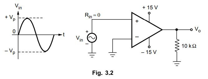
Ans.
:
The circuit acts as a comparator, with noninverting comparator,
Vref=
0V. When Vin > 0, Vo changes from Vsat to + Vsat
and when Vin < 0, Vo changes from +Vsat to
- Vsat. Assuming Vsat = ± 15 V, the output + = waveform
is as shown in the Fig. 3.3. This is also called noninverting zero crossing
detector.

Q.112
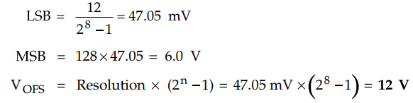
Calculate the values of the LSB, MSB and full scale output for an 8-bit DAC for
the 0 to 12 V range.
Ans
:
Q.113
An 8-bit A/D converter has an input range 0-3 volt. Calculate the minimum
voltage it can resolve. May-04
Ans.
:
Minimum voltage = 3 / 28-1 = 3 / 255 = 0.01 V = 11.76 mV
Q.114 A 10 bit A/D converter has an input voltage of -10 to + 10 V. Find resolution.
Ans.
:
Resolution = ViFs / 2n – 1 = 20 / 210 – 1 =
0.019550
Q.115
A 4 bit resistance ladder has resistor values of R = 10 k and 2 R = 20 kn. Vref=
10 V. Find the resolution of the ladder and lout for a digital input of 1111.
Ans:

Q.116
What are the applications of peak detectors ?
Ans.
:
1. Test and measurement instrumentation systems
2.
In amplitude modulation (AM) in communication systems.
3.
In fibre optic receivers.
4.
A circuit driving flash of a camera.
5
In various signal processing circuits.
Q.117
How many resistors are required in a 12-bit weighted resistor DAC ?
Ans.
:
Thirteen resistors are required in a 12-bit weighted resistor DAC. One resistor
for each bit and one feedback resistor (Rf).
Q.118
Why integrating type ADC's are preferavly used for DC and slow varying signals?
Ans.
:
Integrating type ADC's such as single slope and dual slope ADCs are slow-speed
type ADCs and hence they are preferably used for DC and slow varying signals.
Q.119
In circuit shown in above figure, calculate Vo, ACL, load
current iL and output current Io.
Ans.
:
It is inverting amplifier.

Q.120
Draw the circuit of a log amplifier using two op-amps
Ans.
Refer
Fig. 3.2.2 of section 3.2.2.
Q.121
Calculate the numver of comparators required for realizing an 8-bit flash A/D
converter. May-15
Ans.
:
8 number of comparators.
Q.122
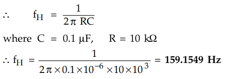
Calculate the cut-off frequency of the first order active filter shown in Fig.
3.6.
May-04

Ans.
:
The given filter is first order low pass filter.
Q.123
What is the advantage of using active clipper over passive clipper ?
May-16,
Dec.-16
Ans.
:
The advantages of active clipper are,
1.
Flexible design
2.
High accuracy of clipping
3.
Less components producing noise.
4.
Gives isolation between input circuits and load circuits.
Q.124
Draw the circuit diagram of a zero cross detector with input and output
waveforms.
May-17
Ans.
:
The Fig. 3.7 shows inverting zero crossing detector which is nothing but
inverting comparator with zero reference voltage.

Q.125
Write any two applications of clipper and clamper.
Ans.:
The applications of clipper are,
1.
In speech processing for communication applications
2.
In pulse height analyzers.
3.
In television and FM receivers.
The
applications of clamper are,
1.
As a d.c. restorer circuit in t.v. receivers.
2.
In cameras for the flash circuit.
3. In radar and sonar circuits.
Linear Integrated Circuits: Unit III: Applications of Op-amp : Tag: : Applications of Op-amp | Linear Integrated Circuits - Two Marks Questions with Answers
Related Topics
Related Subjects

Linear Integrated Circuits
EE3402 Lic Operational Amplifiers 4th Semester EEE Dept | 2021 Regulation | 4th Semester EEE Dept 2021 Regulation