Microprocessors and Microcontrollers: Unit V: (b) Introduction to RISC Based Architecture
Two Marks Questions with Answers
Microprocessors and Microcontrollers: Unit V: (b) Introduction to RISC Based Architecture : Two Marks Questions with Answers
Two Marks Questions with Answers
Q.1
What is CCP Module?
Ans.
: The CCP (Capture/Compare/PWM) module contains a 16-bit register that
can operate as a 16-bit Capture register, as a 16-bit compare register or as a
PWM duty cycle register.
Q.2
What is difference between CCP and ECCP module?
Ans.
: The operation of the ECCP module is identical to that of the CCP module.
The ECCP module, on the other hand, has Enhanced PWM functionality and
auto-shutdown capability.
Q.3
What is CAN module?
Ans.
: The Controller Area Network (CAN) module is a serial interface, useful
for communicating with other peripherals or microcontroller devices. This
interface/protocol was designed to allow communications within noisy
environments.
Q.4
What is MSSP module?
Ans.
: The Master Synchronous Serial Port (MSSP) module is a serial interface
useful for communicating with other peripheral or microcontroller devices. It
has two modes of operation:
•
3-wire SPI (Supports all 4 SPI modes)
•
I2C Master and Slave mode
Q.5
What USART module?
Ans.
: The Universal Synchronous Asynchronous Receiver Transmitter. (USART)
is a serial interface that can be configured in the following modes:
•
Asynchronous (full-duplex)
•
Synchronous - Master (half-duplex)
•
Synchronous - Slave (half-duplex)
Q.6
What is W register?
Ans.
: It
is 8-bits wide. It is used for ALU operations. The WREG register is the same as
the accumulator in other microprocessors. The contents of WREG register are
used for all arithmetic and logic one/ two- operand instructions. It is not an
addressable register.
Q.7
Draw the bit pattern of status register of PIC18.
Ans.
:

Q.8
What is File register in PIC18?
Ans.
:
In PIC18 microcontrollers, the data (Read/Write) memory is implemented as
static RAM. It is also known as File Register. Like WREG we can perform
arithmetic and logic operations on many locations of the file register data
RAM.
Q.9
What is access bank?
Ans.
: The access bank is comprised of the upper 160 bytes in Bank 15 (SFRs)
and the lower 96 bytes in Bank 0. These two sections will be referred to as
Access Bank High and Access Bank Low, respectively.
Q.10
List the addressing modes supported by PIC18 microcontroller.
Ans:
The PIC 18 microcontroller supports following addressing modes:
1.
Immediate addressing mode
3.
Register indirect addressing mode
2.
Direct addressing mode
4.
Register Indirect/Indexed ROM addressing mode
Q.11
List the I/O ports supported by PIC18F458.
Ans.
: The PIC18F458 has five I/O ports:
•
Port A (7- Bit): RAO RA6
•
Port B (8-Bit) : RBO - RB7
•
Port C (8- Bit): RCO - RC7
•
Port D (8-Bit): RD0 - RD7
•
Port E (3- Bit): REO - RE2
Q.12
List the SFRS associated with each Port in PIC 18.
Ans.
: Each
port has three Special function registers (SFRS) associated with it:
•
TRIS register (Data Direction register)
•
PORT register (reads the levels on the pins of the device)
•
LAT register (output latch)
Q.13
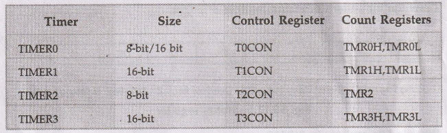
State the timers available in PIC18F458
Ans.
: PIC18F458
has four timers. The timers 0, 1 and 3 are 16-bit timers while timer 2 is
8-bit timer. These timers can be used as timer, counters or for PWM generation.
Q.14
State the sources of interrupts in PIC18.
Ans.
: The PIC18 devices have multiple interrupt sources depending on which
peripherals are incorporated in the chip. Some of the most widely used
interrupt sources of PIC18 are:
External
Hardware interrupts : INTO, INT1 and INT2
•
Timer interrupts : TMROIF, TMR1IF, TMR2IF,and TMR3IF
•
Serial Communication Interrupts : TXIF and RCIF
•
RB Port Change interrupt: RBIF
•
A/D Converter interrupt: ADIF
•
Compare, Capture, PWM interrupt : CCP1IF
Microprocessors and Microcontrollers: Unit V: (b) Introduction to RISC Based Architecture : Tag: : - Two Marks Questions with Answers